Analysts support Intel's claim that Moore's law in the chip industry has not failed

[NetEase Smart News, April 3] In the past few years, there have been many stories about how Moore's Law has failed or is about to end. This is one reason for the panic in the financial world because it shows that technological progress is slowing and the global economy may be affected.
It's just not true. The Honorary Chairman of Intel Corporation Gordon Moore predicted in 1965 that the number of transistors in the same volume chip would double every few years. The magic of this law has been for decades, but as Intel silences its chip development progress, this law seems to have slowed down. But last week, Intel disclosed that although the company took longer to achieve the latest technological leap, its 10-nanometer process micro-transistor was far more than expected. This means that Moore's Law is still valid.
Intel plans to convert its 14-nm manufacturing process into a 10-nanometer manufacturing process later this year. One nanometer is one-billionth of a meter. This number represents the spacing between circuits in the chip. Intel said that its manufacturing process is ahead of competitors such as Samsung, TSMC and Global Foundries.
At Intel's conference, I saw Dan Hutcheson, CEO of VLSI Research, a market research company. For decades, Hutcheson has been focusing on reporting on the chip industry. I also interviewed him on Intel’s assertions. The following is an edited conversation record.
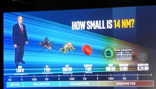
Figure: Intel's view of the microchip circuit
VentureBeat: How do you think about the tenacity of the 10-nanometer process?
Dan Hutcheson: Let's start with the current nanometer process. This topic can be traced back to the 1990s. Before that, everyone used dynamic random access memory (DRAM). I don't know if anyone will remember. Then, dynamic random access memory is the Japanese world. Well, we are not leading in the DRAM field. So how do we come up with some of the leading technologies that apply to us? That is the emergence of nano nodes. Although we called them micron at that time. After some time, we only turned to nano.
VB: In Intel's statement, they have a three-year leading edge in technology. Does this make sense? They said that their 14-nanometer process is equivalent to what other people call 10 nanometers?
Hutcheson: Oh, that's it. This is the case for a long time, from 40 nm or 65 nm. Intel leads all competitors. A few years ago, they had a lot of lead. After developing nano-chip manufacturing processes, they slowed down.
VB: Everyone is worried about the slowdown of Moore's Law.
Hutcheson: This is all shit. These are all opponents who are unable to compete, so they discuss how Moore's Law will die. I have written two articles to discuss whether Moore's Law has already died. One of them was in 1996. The other article was in 2005, or I think it was in 2003. This topic is constantly being debated in the industry. I have found an article published in 1968 that Moore's Law will die. Even Gordon himself stated in a 1965 paper that he believes that Moore's Law will only last until the 1970s.
VB: This may be a strategy. AMD has been saying that since Moore's Law is slowing down, Intel’s leading edge in this area is no longer that big. And their zen chip will have a greater impact. They can say that Intel cannot surpass them. Or this is their point of view.
Hutcheson: The advantage of AMD has always been design. If you go back to the 130-nm age, AMD's manufacturing process is more stringent than Intel's. But this is no longer a fact. But the slowdown in Moore's Law is their fiction. In my memory, the way people look at Moore's Law is, how many transistors can I put into a chip, but only half the price? You can easily measure it by Rayleigh distribution. It ultimately boils down to whoever has the relevant manufacturing tools. They tell you that they are technically capable at any given time.
The problem is that if you and I both drive Ferrari at the Sonoma track and Formula One driver Sebastian Vettel is also in the same car, he will circle around us. This is what Intel described today. They like to jump out and say, "We are still producing faster laptops."
VB: Qualcomm's point of view is that their growth curve in smart phone chip production is very good, but Intel does not, so when Intel's personal computer business slows down, their mobile chip development speed is faster. Earlier this year they released their own 10-nanometer chip.
Hutcheson: In fact, every company deliberately hides their 10-nanometer chip and is not really 10 nanometers. Just like you said that you are 20 years old and not really 20 years old.
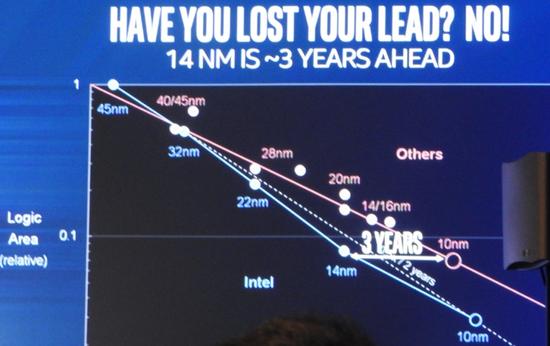
Figure: Intel's manufacturing process is shown in blue, while competitors are shown in red.
VB: What does a concept like "gate length" tell you? What does this indicator tell you?
Hutcheson: This can be attributed to the size of the static random access memory SRAM cell. I'm still observing in such a way that if I look at the size of the units these guys publish at the International Electronic Equipment Conference, you can see where they are in the market competition. Because you can't directly compare the PC chip with the server chip, because the density will be different, depending on how you use the transistor, priority is given to performance or energy consumption. Again, how many SRAM cells you need depends entirely on your application. SRAM is very intensive in form. But the logic is very loose. Things like input and output are very loose. According to your needs, you will get different chip density. You might say, "What is the smallest unit?" This is the standard that Intel has been using: the minimum height and width we can make on each cell. But this is not a good measure.
Our other problem is that the new naming does not have a convention. This is just how you call it.
VB: Does it sound like these manufacturing companies are not very rigorous? Will they use a 10 nanometer manufacturing process?
Hutcheson: Well, for the entire chip manufacturing industry, they are very serious about the 10-nanometer process. This is their biggest advantage. So how do they integrate their capabilities into design and link manufacturing processes with design to gain a competitive advantage?
In your opinion, Qualcomm said they are leading in this area. In fact, they are really leading the CDMA related technologies and patents. No matter what the transistors in the chip are, they have the core technology to make them lead. Transistors are just the beginning for Qualcomm. Even if there is no competitive advantage in the transistor, it can still be compensated by other aspects. The difficulty is, how do you make up for differences in functionality? It is critical for mobile devices because if your modem is using more power, you lose. You need to make your battery life stronger.
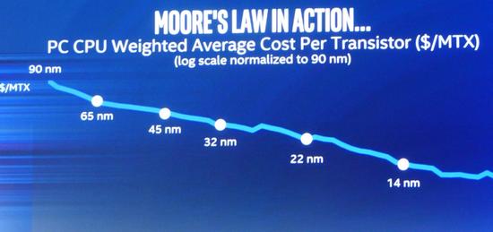
Figure: Moore's Law still exists, but it will not always be stable.
VB: There is not much discussion about power consumption today. Is this something you need to know more about?
Hutcheson: This is more like a dark art. They talked a bit about 22 nm, 10 nm, and 14 nm processes, and why they were kicking out the 22 nm process for low power. The key is that when you are primarily looking for ultra-low power, you will choose a different architecture, different transistors. The entire design process will be based on a completely different starting point.
VB: How do they view 3D Xpoint this new technology?
Hutcheson: They are two different concepts within Intel. 3D Xpoint is mainly about storage. I suspect that in the future you will see that 3D Xpoint may be integrated in a different way, but before the introduction of Xpoint, it would make more sense to do different integrations on DRAM.
VB: Is this a lot of different types of packaging products?
Hutcheson: Yes. Fundamentally, I need to provide processor information. The fastest to input information to the processor is SRAM, then DRAM, and flash again. The current situation is that the gap between flash and DRAM is increasing. Xpoint access speed is exactly between the two. My feeling is that they are not yet ready to integrate 3D Xpoint. More meaningfully, DRAM is integrated on a micron-sized chip. If you look at what Micron is talking about, it's mainly about system package integration level and embedded DRAM, which will be packaged into different products. Someone bought this kind of DRAM from them and then integrated it with other chips.
VB: Go back to Moore's Law. If they take longer to reach 10 nanometers, but they have a 2.7-fold improvement, not just a 2-fold improvement, is that still Moore's Law? This is a way of Moore's Law ?
Hutcheson: We are still in Moore's law. As long as you can double your performance every few years, you are still in the circle of Moore's Law. This is not the end. In fact, what you see is a debate about Moore's Law, sometimes purely exaggerated speech. People are accustomed to drawing on John Chen's forecasting chart, saying Moore's Law is declining. People still refer to this chart, but now they use it as a historical reference. This is just a prediction. On the day of its publication, John Chen said: "If we don't do something, it will really do so." This chart was re-mentioned after a year or two, and people have used it since then. Say: "Look, it is dying."
This is not just Intel's compliance with this law of development. You can also look at Taiwan Semiconductor Manufacturing Co., and their chip density is still twice that of the original, as is Global Foundries. However, the remarks on the slowdown in Moore's law are still very popular. (English source /venturebeat compiler / machine Xiaoyi proofread / æ™— ice)

In fact, what people usually call a pinhole camera does not use a pinhole lens. Pinhole lens refers to a lens that uses the principle of small hole imaging to obtain images. It is inexpensive and simple in principle, but its fatal weakness is that too little light passes through the small hole, resulting in too long exposure time. Taking photos with a pinhole lens in sunlight can take anywhere from a few minutes to a dozen minutes, especially when shooting at night with exposure times of up to several hours. Obviously, for a camera that shoots dozens to dozens of frames per second, it cannot meet the requirements. Pinhole lenses cannot be applied to cameras, so there is no "pinhole" camera in the strict sense. As is customary, a miniature camera using a fisheye lens, a flat lens or a conical lens is called a pinhole camera.
According to the lens, the lens of the pinhole camera can be divided into three types: fisheye lens, flat lens and conical lens; according to the photosensitive element used, it can be divided into charge coupled element and complementary metal oxide semiconductor; According to the data transmission method, it can be divided into two categories: wireless cameras and wired cameras.
Jingjiang Gisen Technology Co.,Ltd , https://www.gisengroup.com