
The audio amplification circuit diagram of LM386 has one chip in everyone's mind. You know it very well. The typical application circuit is familiar with the chest. Once you have some kind of demand, you can think of it immediately, although it may not be the best for completing the task. Choice, but you can't give up on it, this is feelings. Different people have different answers, but for analog audio amplification, this chip is LM386. 
Figure 1 LM386 chip
As a piece of old-age chip, LM386 has been produced because of its excellent design ideas. 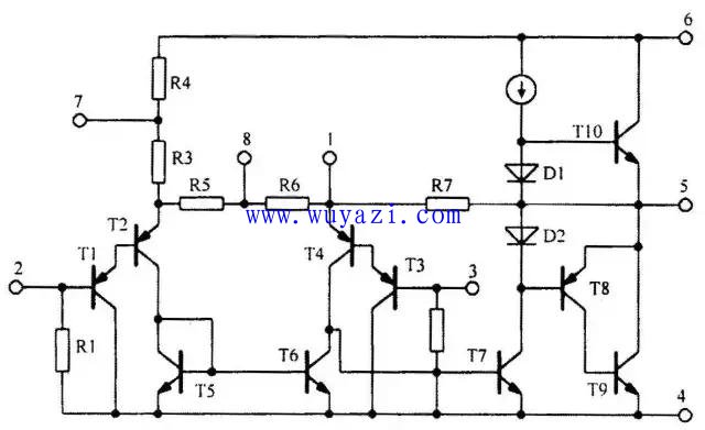
Figure 2 The first stage of the internal structure of LM386 is a differential amplifier circuit. T1 and T2, T3 and T4 respectively form a composite tube as the amplification tube of the differential amplifier circuit; T5 and T6 form the mirror current source as the active load of T1 and T3; The input signal is input from the base of the T1 and T3 tubes, and the collector output of the T4 tube is a double-ended input single-ended output differential circuit. Using a current source as the active load allows the gain of the single-ended output circuit to be approximately equal to the gain of the double-ended output.
The second stage is a common-emitter amplifier circuit, and T7 is an amplifying tube, and a constant current source is used as an active load to increase the voltage amplification factor of the current stage.
The T8 and T9 in the third stage are combined into a PNP type tube, and the NPN type tube T10 constitutes a quasi-complementary output stage. Diodes D1 and D2 provide the appropriate bias voltage for the output stage to eliminate crossover distortion.
Pin 2 is the inverting input and pin 3 is the non-inverting input. The circuit is powered by a single power supply and is therefore an OTL circuit. The output (pin 5) needs to be connected to the load via a capacitor.
Resistor R7 is connected from the output to the emitter of T4 to form a feedback path, and forms a feedback network with R5 and R6 to form a deep voltage series negative feedback to stabilize the voltage gain of the entire circuit.
LM386 features low static power consumption, about 4mA, can be used for battery power supply operating voltage range, 4-12V or 5-18V
Adjustable external component with less voltage gain, 20-200dB
Low distortion 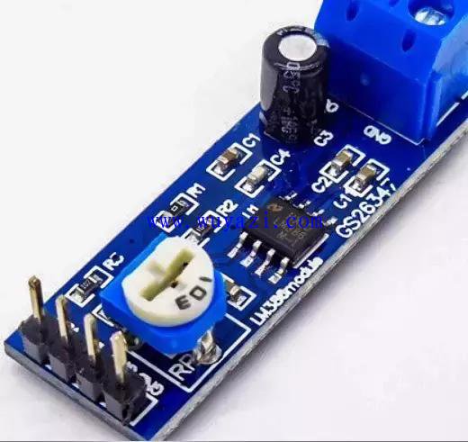
Figure 3: The audio amplifier circuit composed of LM386 can easily form an audio amplifier circuit by LM386. The circuit of Figure 4 requires the least components, the voltage gain is 20dB, and the voltage gain of the circuit shown in Figure 5 can be up to 200dB. 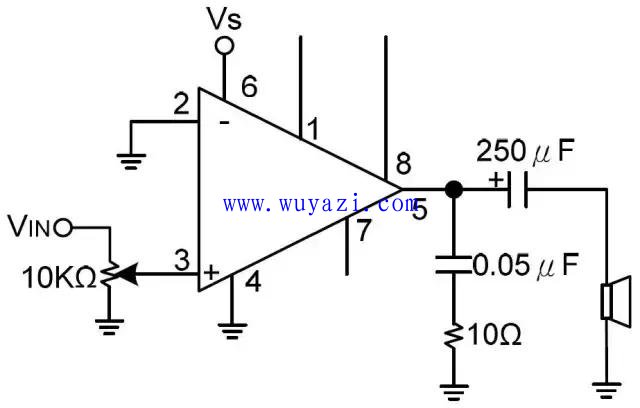
Figure 4 Amplifier gain = 20 (minimum components) 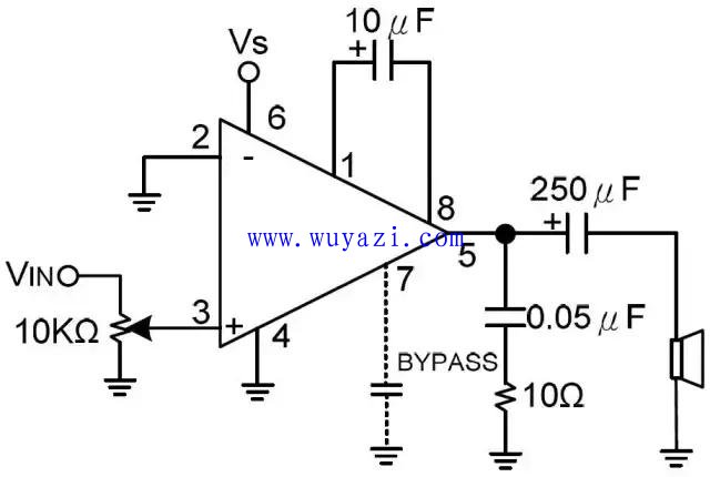
Figure 5 amplifier gain = 200
According to the data sheet, the LM386 operates at 4-12V or 5-18V (LM386N-4) with a static current consumption of 4mA and a voltage gain of 20-200dB. When the 1 and 8 feet are open, the bandwidth is 300KHz; the input impedance is 50 kΩ, and the audio power is 0.5W. Although the application of LM386 is very simple, but pay attention to it, especially when the device is powered on, power off, or even after the work is stable, some operations (such as plugging and unplugging the audio plug, rotating the volume control) will bring the transient impact. Very annoying noise is generated on the output speaker.
The gain is changed by a capacitor connected between pin 1 and pin 8 (1 pin capacitor + pole), and the gain is 20 dB when disconnected. Therefore, without using a large gain, the capacitor is not connected, not only saves cost, but also reduces noise.
When designing the PCB, all the peripheral components should be as close as possible to the LM386, the ground wire should be as thick as possible, and the input audio signal path should be as parallel as possible, and the output should be the same.
Choose the potentiometer to adjust the volume, the quality is too bad, otherwise the victim is the ear; the resistance is not too big, 10K is the most suitable, too much will affect the sound quality, turn so many circles, annoying!
Use dual audio input/output whenever possible. The advantage is that the "+" and "-" outputs can cancel the common mode signal well and effectively suppress common mode noise.
The bypass capacitor of the 7th pin (BYPASS) is indispensable. In practical applications, the BYPASS terminal needs an external electrolytic capacitor to the ground to filter out noise. After the operation is stable, the voltage of the pin is approximately equal to half of the power supply voltage. Increase the capacitance of this capacitor, slow down the rise and fall speed of the DC reference voltage, and effectively suppress noise. The noise when the device is powered on or off is caused by the instantaneous jump of the bias voltage. This capacitor can be saved!
Reduce the output coupling capacitance. The function of this capacitor is: DC + coupling. Blocking the DC voltage, if the DC voltage is too large, it may damage the speaker coil; the AC signal of the coupled audio. It forms a first-order high-pass filter with the speaker load. Reducing the capacitance value makes the amplitude of the noise energy impact smaller and the width narrower; too low also increases the cutoff frequency (fc=1/(2Ï€*RL*Cout)). The test found that 10uF/4.7uF is more suitable.
There are a lot of well-designed LM386 practice kits and modules. A well-funded student can consider buying a set and study it carefully. The circuit is very simple, but the analog circuit adjustment is still somewhat difficult and requires a certain amount of experience to accumulate. It is worthwhile for beginners to practice.
The output of the LM386 is connected to the speaker. If there is no check on the hand, the price can range from a few cents to a few dollars. The input can be connected to various sources, or you can use the electret microphone as your input signal. If conditions permit, it is recommended to use the signal generator as input, use the oscilloscope to observe the input and output waveforms, and check the amplification factor of the circuit and the degree of distortion of the signal.
The electret microphone consists of two parts: acoustic and electrical conversion and impedance transformation. The key component of acoustic-electric conversion is the electret diaphragm. It is a very thin plastic film with a thin metal film on one side. Then, after passing through the high-voltage electric field, the opposite sides are respectively charged with opposite charges. The vaporized gold of the diaphragm faces outward and communicates with the metal casing. In the electret microphone, there is a FET for pre-amplification, so the electret microphone needs a certain bias voltage during normal operation. This bias voltage is generally not more than 10V. 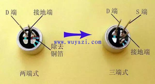
Figure 7 electret microphone 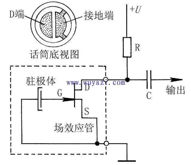
Figure 8 Electret Microphone Circuit Connection For beginners in freshman and sophomore, in addition to experimenting on the breadboard, it is recommended to draw the schematic and PCB board with Altium Designer software, and try to make the board fun. Regarding the use of Altium Designer, there are a lot of video tutorials on the Internet, and I will slowly explore it.
Dongguan Guancheng Precision Plastic Manufacturing Co., Ltd. , https://www.dpowergo.com