
Abstract: A solution for data collection and storage system based on SOPC technology is proposed. The system realizes its hardware circuit by configuring a micro-blaze soft core processor, user-defined data acquisition and storage interface logic, USB transmission module and bus interface module on a Xilinx Spartan 3E series FPGA chip. The data acquisition system can measure multiple signals at the same time and has a large storage capacity. Due to the use of SOPC technology, the system has the advantages of flexible design, high integration, small size and low power consumption.
Introduction: With the continuous development of integrated circuits, programmable logic device FPGA has been more and more widely used due to its powerful functions, flexible design, short development cycle and other characteristics. Therefore, the design method of the System On Programmable Chip (SOPC) has also received more and more attention. SOPC integrates functional modules necessary for system design such as microprocessors, memories, timers, and general-purpose I / O interfaces, as well as user-designed modules with specific functions, into a programmable logic device to build a software and hardware Programmable system-on-chip for programming functions. This very flexible circuit design makes it easy to cut, expand, and upgrade the entire circuit system. This can shorten the development cycle of the circuit design and save development costs.
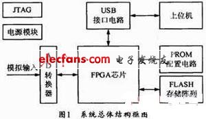
1 Overall system structure
The whole system consists of spartan3E high-performance, low-cost 90nm FPGA of xilinx company and some peripheral circuits. There are mainly AD converter, FLASH memory, system PROM configuration circuit and power module, etc. The overall structure of the system is shown in Figure 1.
The system core adopts embedded technology and is implemented on a chip. It contains Xilinx's standard bus IP cores such as interrupt controllers, general input and output ports and other modules and user-defined data acquisition and storage IP with PLB bus interface. nuclear. The user-defined IP core is designed in VHDL language, which contains AD control logic, FLASH control logic, DMA transmission control logic and FIFO buffer module.
The entire system design can be divided into hardware design and software design. Using SOPC technology and VHDL hardware description language to design a hardware control system inside the chip; using EDK (embedded development kit) to automatically generate a software package for a specific hardware configuration combined with C language to design a software control program based on Microblaze processor.
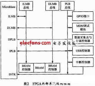
2 System structure
The hardware design of the FPGA first determines the external interface to be used, and then performs the IP core design to map the logic functions of the IP core to the FPGA chip. Its system structure block diagram is shown as in Fig. 2.
2.1 AD conversion chip
The AD converter uses MAXIM's MAXIM1308 chip. It is a 12-bit analog-to-digital converter (ADC) that provides 8 independent input channels. An independent sample-and-hold (T / H) circuit provides simultaneous sampling for each channel and provides a + 5V input. Range, 20MHz, 12-bit bidirectional parallel data bus is used to provide conversion results, and can accept digital input to individually configure the opening and closing of each channel.
2.2 FLASH memory
The FLASH memory chip uses 8 pieces of Samsung's K9XXG08UXA series of NAND Flash memory. The memory is read and written by page and erased by block, and commands / addresses / data are sent through I / O pins in a time-multiplexed manner. The storage capacity of each piece is 512MB. Stored procedures use pipelined methods to store data.
Interface Encoders Decoders Converters
Interface Encoders Decoders Converters,Integrated Circuit Oem Dip Original,Temperature Sensor Ic,Pptc Resettable Circuit Protection Fuse
Shenzhen Kaixuanye Technology Co., Ltd. , https://www.icoilne.com