introduction
Multi-node systems can be seen in many current electronic system applications. This multi-node system is more and more widely used due to its structural scalability, flexibility in function configuration, and easy maintenance of faulty nodes. In general, the main hardware components of each node of a multi-node system have great similarities. In particular, in recent years, FPGA, a powerful platform, has made the hardware components of multi-node systems more widely versatile. Especially with the promotion of IP core technology, coupled with the emergence of some powerful CPU cores, such as PicoBlaze and MicroBlaze provided by Xilinx, the main functions of many current systems can be realized by large-capacity FPGAs. No need to use more expensive high-performance microprocessors.
For node systems, this will greatly reduce system cost. For multi-node systems consisting of high-capacity FPGAs, system upgrades are a time-consuming and laborious task. At this point, the remote upgrade capability of the FPGA is particularly important. For multi-node systems including high-performance embedded microprocessors such as ARM, DSP, PowerPC, these embedded microprocessors are used to load and remotely upgrade the FPGA with SELECTMAP, which is very economical and efficient without adding too many external components. of. However, for a core device that is a high-capacity FPGA system, if the FPGA itself receives the upgrade data and writes the non-volatile memory that stores the configuration data, once the upgrade fails, it will not be upgraded again, which limits its high reliability in many cases. Sexual requirements or applications where maintenance personnel are inconvenient to reach; and the addition of expensive embedded microprocessors simply to achieve remote upgrades of the system will increase system cost and complexity. In response to this situation, the author designed a remote upgrade system consisting of ATmega64 microcontroller and RS485 bus, plus the main control computer connected to the Ethernet, to solve the above problems.
1 system design
1.1 System Structure Design
The remote upgrade system is mainly composed of a main control computer connected to the Ethernet, a half-duplex RS485 bus and various sub-nodes. The composition is shown in Figure 1. The main control computer obtains the upgrade data of each node of the whole system from the external through Ethernet, and then sends its corresponding upgrade data to each sub-node through the RS485 bus to complete the upgrade of the multi-node system. The RS485 bus adopts a master-slave half-duplex mode. The master computer is the main controller of the bus. It can only initiate communication connections to each node. The other child nodes can only respond to the control commands of the master computer.

Figure 1 Block diagram of a multi-node high-capacity FPGA system remote upgrade system
1.2 Node Upgrade Principle
Each node is connected to the main control computer through the RS485 bus. When there is no upgrade data, the bus can be used to transmit the query and control commands of the main control computer to each node. The communication protocol between the master computer and each node may adopt a protocol having three types of frame: a query control frame, a response frame, and a data frame. Only the master computer can send query control frames, query or set the remote upgrade status or working condition information of each node. The child node receives the command and data of the master computer, sends the response frame, and completes its own upgrade.
2 child node hardware design
2.1 Subnode hardware structure block diagram
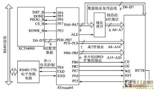
As shown in Figure 2, taking a system consisting of Xilinx's XC3S4000 high-capacity FPGA as an example, the hardware circuits of the remote upgrade system sub-node mainly include: ATmega64 MCU, Flash for storing large-capacity FPGA configuration data, and access Half-duplex bus transceiver for RS485 bus. The ATmega64 microcontroller is used to load the high-capacity FPGA XC3S4000, and receive the FPGA upgrade data from the RS485 bus and write it to the Flash memory SST36VF1601C with 2 MB of storage space. The RS485TTL level conversion circuit uses the RS485 transceiver SP485R.

Figure 2 sub-node hardware block diagram
Infrared Pen,Infrared Touch Pen,Infrared Tablet Stylus Pen,Infrared Stylus Pencil
Shenzhen Ruidian Technology CO., Ltd , https://www.szwisonen.com
