
White LED lighting has been widely recognized by everyone for its high efficiency, low power consumption, energy saving and environmental protection. In essence, an LED is a illuminable diode whose luminous intensity is proportional to the forward current passing through it and has a turn-on voltage. When the current is 20 mA, the forward voltage drop is generally 3 to 3.5 V. . In many cases, the luminous intensity of a single LED does not meet the needs of practical applications. It is also necessary to use multiple LEDs in series or in parallel, which requires a large voltage or current to drive, and different manufacturing processes, even different batches, LEDs There is a problem of performance mismatch, which also poses a problem for rational design drive. Therefore, although there are many types of original power supplies, they cannot directly supply power to the LEDs. This requires a boost or buck according to different needs, as well as a constant current or constant voltage drive.
1 Common LED driver working principle
1.1 Linear Regulator Driver
The earliest set of linear regulator drivers appeared in the 1970s, when the NPN tube was used as a voltage regulator device, as shown in Figure 1. This regulator requires 2Vbe between the input voltage and the output voltage. When the input voltage is lower than 2Vbe, the NPN tube becomes saturated and the regulator loses its regulation capability. In order to reduce the pressure difference, a combined regulator has appeared. As shown in Fig. 2, the base of the NPN tube is driven by a PNP tube, but the pressure difference is also close to 1 Vbe. In the mid-1980s, low-dropout linear regulators appeared on the market, as shown in Figure 3. Unlike the NPN regulator, the PNP regulator voltage difference is not a function of Vbe, but a function of the PNP tube Vce. This voltage value is much lower. As the manufacturing process matures, the PNP regulator voltage difference is less than 500. mV.
A linear regulator driver is a transistor that operates in a linear or saturation region. The FET removes excess voltage from the input voltage, producing an adjustable, stable, and accurate DC voltage, usually by a voltage regulator, error amplifier, and feedback. Circuit and reference voltage components. The voltage regulator device is usually a MOS transistor, which is equivalent to a voltage-controlled resistor, and the gate voltage controls the size of the resistor. The output voltage Vout is Vout=Vin-Vp obtained by the voltage divider device and the load divider. If the input voltage Vin or the load changes, the control terminal voltage Vc also changes, and the MOS tube resistance value is controlled to adjust the MOS tube voltage division. The purpose of the Vp size is to make Vout stable. The linear regulator driver can also be connected in series with the load. The feedback voltage Vo=Iout×R1 keeps the R1 size unchanged. The feedback voltage can reflect the change of the output current, and then change to a linear steady current driver. The principle of operation is basically the same as that of a linear regulator driver.
The efficiency of a linear regulator is relatively low. It can be known from the principle that the output voltage of the driver is obtained by subtracting the MOS tube voltage division Vp from the input voltage, and this part of the voltage is completely converted into heat energy consumption. Therefore, in order to improve the driver efficiency, it is generally required that the Vp is as low as possible. A linear regulator driver with a low input/output voltage difference is called a low dropout linear regulator, or LDO for short.
1.2 Charge Pump Driver
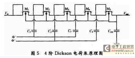
The earliest ideal charge pump model was proposed by Dickson J in 1976. As shown in Figure 5, the basic idea is to generate high voltage through the accumulation effect of capacitance on the charge. Later, Witte-rs J, Toru Tranzawa and others improved the charge pump model of Dickson J, and proposed a more accurate theoretical model, which was confirmed by experiments.
The modern charge pump mainly realizes DC-DC conversion by switch array, oscillating circuit, logic circuit and comparator. The driving mode is also changed from the previous single mode to the adaptive multi-mode. The main form is single mode (such as 2X mode). In dual mode (such as 1X/2X mode) and multi-mode (such as 1X/1.5X/2X mode), the following two-mode 1X/2X charge pump is used to analyze the working principle of the charge pump.
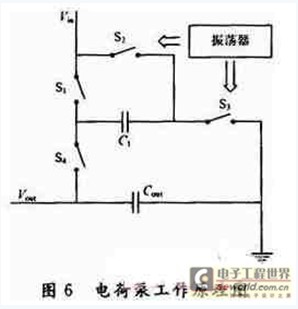
As shown in Figure 6, when the charge pump operates in 1X mode, the oscillator does not work, S1 and S4 are directly turned on, at this time, Vin = Vout; when the charge pump operates in 2X mode, the oscillator output is occupied. The ratio is 50% square wave, so that S1, S3 and S2, S4 are turned on in turn. When the clock signal is high, S1 and S3 are turned on, S2 and S4 are turned off, Vin is connected to C1, and C1 is charged to make Vc =Vin; when the clock signal is low, S1 and S3 are disconnected, S2 and S4 is turned on, Vin is externally powered by C1, so when there is steady state, Vout=Vin+Vc=2Vin.
The charge pump driver circuit not only can effectively boost the buck output, but also can easily carry out the negative voltage output, which is a big advantage of the charge pump driver compared to the other two drivers.
As shown in Figure 7, its basic principle is consistent with the Dickson charge pump, but the voltage difference across the capacitor does not jump. When the circuit is kept in charge and discharge, the voltage difference across the capacitor remains constant. In this case, the original high potential terminal is grounded, so that a negative voltage output can be obtained.
 .
.
Where: Pin is the total input power; Lout is the total current flowing through the load LED; VLED is the forward voltage drop of the LED; M is the boosting multiple of the charge pump; Iq is the drive current of the charge pump power tube and other modules Static current. It can be seen from the above equation that the larger the boosting factor M of the charge pump is, the lower the conversion efficiency of the charge pump is. Therefore, under the condition that the LED driving voltage, that is, Vout>VLED, is satisfied, the charge pump should be operated as low as possible. In the mode of multiples.
1.3 Inductive Switching Regulator Driver
The inductive switching regulator driver is called Switching Power Supply. It is named because the device that adjusts the voltage regulation function in the power supply always works in the switching mode. The early switching power supply frequency was only a few kilohertz. When the frequency reached about 10 kHz, the magnetic components such as transformers and inductors emitted very harsh noise. Until the 1970s, the switching frequency broke the 20 kHz of the human ear's hearing limit. The problem is solved. As the switching frequency continues to increase, the size of the drive is reduced and the efficiency is improved. In the 1980s, zero-voltage and zero-current switching circuits using quasi-resonant technology, namely soft-switching technology, emerged. This circuit makes the voltage and current before the switch is turned on or off is zero, which solves the switching loss and switching noise problem in the circuit, so that the switching frequency can be greatly improved, so that the switching power supply is further small in size and light in weight. High efficiency and high power density.
The core of the inductive switching regulator driver is the electronic switching circuit. According to the output voltage regulation or steady current characteristics of the power supply, the feedback control circuit is used to control the switching circuit. When the switch tube is closed, the energy of the power source is stored in the inductor. When the switch tube is turned off, the energy in the inductor flows into the capacitor, thus realizing the transmission of energy.
The inductive switching regulator driver has two common control modes: one is to maintain the switching cycle of the switch, and the pulse width modulation mode (PWM) that controls the on-time of the switch. When the input voltage or load changes, the control circuit passes. Closed-loop feedback of the difference between the output voltage or current and the reference voltage, adjusting the on-pulse width of the main circuit switching device, so that the output voltage or current of the inductive switching regulator driver remains stable; the other is to keep the on-time unchanged The pulse frequency modulation mode (PFM) for changing the duty cycle of the switch, the basic working principle is that the control circuit performs closed-loop feedback through the difference between the output voltage and the reference voltage under the condition of input voltage or load change, while keeping the switch open time unchanged. In the case of controlling the length of the switching cycle, that is, controlling the switching frequency, the switching duty ratio is adjusted to achieve the purpose of stabilizing the output voltage or current. Since the PWM mode circuit is simple and the input/output range is wider than the PFM method (PFM is usually used for light load, low voltage, and low current), it has been widely used. The following two types of PWM driving methods are mainly introduced.
1.3.1 Voltage Controlled PWM
The structure diagram is shown in Figure 8.
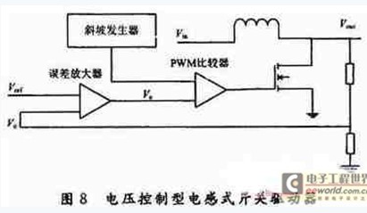
In the PWM controller, the output voltage Vo is detected and applied to the inverting input of the op amp, and the fixed reference voltage Vref is applied to the non-inverting input of the op amp. After the error is amplified, the DC error voltage Ve is output and applied to the non-inverting input of the PWM comparator; the ramp signal generator generates a sawtooth signal Vosc to the inverting input of the PWM comparator. After Vc and Vosc are compared by PWM, a square wave signal is output, and the duty ratio of the square wave signal changes with the error voltage Vc. When the output voltage decreases, the Ve value becomes larger. After the PWM comparison, the output square wave duty ratio decreases, the MOS tube conduction time increases, Vin increases the inductor charging time, and Vout rises.
1.3.2 Current Control PWM Principle
The structure diagram is shown in Figure 9. The difference between the circuit and the voltage control type is that the circuit has two parts of an outer control loop and an inner control loop. When the output current Iout decreases, the error amplifier output increases, the PWM output is 0; when the rising edge of the oscillating wave comes, the MOS transistor is turned on, Vin charges the inductor, the current increases, and the feedback voltage increases through the sampling resistor R3, when the feedback voltage When the value exceeds Ve, the PWM output is 1. When the falling edge of the oscillator comes, the MOS transistor is turned off, and the current on the inductor is output to the outside. The current control mode has the same inverse relationship with the output voltage as the voltage control mode. It also has the following characteristics: the outer control loop controls the current minimum; the inner loop controls the current maximum.

2 Comparison of advantages and disadvantages of various drives
For the LED driving method, each LED driver has its applicable range, and also has its own advantages and disadvantages, to understand their respective advantages and disadvantages, and to better design a reasonable LED driving circuit according to the actual situation, which can be passed Efficiency White LED lighting has been widely recognized by everyone for its high efficiency, low power consumption, energy saving and environmental protection. In essence, an LED is a illuminable diode whose luminous intensity is proportional to the forward current passing through it and has a turn-on voltage. When the current is 20 mA, the forward voltage drop is generally 3 to 3.5 V. . In many cases, the luminous intensity of a single LED does not meet the needs of practical applications. It is also necessary to use multiple LEDs in series or in parallel, which requires a large voltage or current to drive, and different manufacturing processes, even different batches, LEDs There is a problem of performance mismatch, which also poses a problem for rational design drive. Therefore, although there are many types of original power supplies, they cannot directly supply power to the LEDs. This requires a boost or buck according to different needs, as well as a constant current or constant voltage drive.
1 Common LED driver working principle
1.1 Linear Regulator Driver
The earliest set of linear regulator drivers appeared in the 1970s, when the NPN tube was used as a voltage regulator device, as shown in Figure 1. This regulator requires 2Vbe between the input voltage and the output voltage. When the input voltage is lower than 2Vbe, the NPN tube becomes saturated and the regulator loses its regulation capability. In order to reduce the pressure difference, a combined regulator has appeared. As shown in Fig. 2, the base of the NPN tube is driven by a PNP tube, but the pressure difference is also close to 1 Vbe. In the mid-1980s, low-dropout linear regulators appeared on the market, as shown in Figure 3. Unlike the NPN regulator, the PNP regulator voltage difference is not a function of Vbe, but a function of the PNP tube Vce. This voltage value is much lower. As the manufacturing process matures, the PNP regulator voltage difference is less than 500. mV.
A linear regulator driver is a transistor that operates in a linear or saturation region. The FET removes excess voltage from the input voltage, producing an adjustable, stable, and accurate DC voltage, usually by a voltage regulator, error amplifier, and feedback. Circuit and reference voltage components. The voltage regulator device is usually a MOS transistor, which is equivalent to a voltage-controlled resistor, and the gate voltage controls the size of the resistor. The output voltage Vout is Vout=Vin-Vp obtained by the voltage divider device and the load divider. If the input voltage Vin or the load changes, the control terminal voltage Vc also changes, and the MOS tube resistance value is controlled to adjust the MOS tube voltage division. The purpose of the Vp size is to make Vout stable. The linear regulator driver can also be connected in series with the load. The feedback voltage Vo=Iout×R1 keeps the R1 size unchanged. The feedback voltage can reflect the change of the output current, and then change to a linear steady current driver. The principle of operation is basically the same as that of a linear regulator driver.
The efficiency of a linear regulator is relatively low. It can be known from the principle that the output voltage of the driver is obtained by subtracting the MOS tube voltage division Vp from the input voltage, and this part of the voltage is completely converted into heat energy consumption. Therefore, in order to improve the driver efficiency, it is generally required that the Vp is as low as possible. A linear regulator driver with a low input/output voltage difference is called a low dropout linear regulator, or LDO for short.
1.2 Charge Pump Driver
The earliest ideal charge pump model was proposed by Dickson J in 1976. As shown in Figure 5, the basic idea is to generate high voltage through the accumulation effect of capacitance on the charge. Later, Witte-rs J, Toru Tranzawa and others improved the charge pump model of Dickson J, and proposed a more accurate theoretical model, which was confirmed by experiments.
The modern charge pump mainly realizes DC-DC conversion by switch array, oscillating circuit, logic circuit and comparator. The driving mode is also changed from the previous single mode to the adaptive multi-mode. The main form is single mode (such as 2X mode). In dual mode (such as 1X/2X mode) and multi-mode (such as 1X/1.5X/2X mode), the following two-mode 1X/2X charge pump is used to analyze the working principle of the charge pump.
As shown in Figure 6, when the charge pump operates in 1X mode, the oscillator does not work, S1 and S4 are directly turned on, at this time, Vin = Vout; when the charge pump operates in 2X mode, the oscillator output is occupied. The ratio is 50% square wave, so that S1, S3 and S2, S4 are turned on in turn. When the clock signal is high, S1 and S3 are turned on, S2 and S4 are turned off, Vin is connected to C1, and C1 is charged to make Vc =Vin; when the clock signal is low, S1 and S3 are disconnected, S2 and S4 is turned on, Vin is externally powered by C1, so when there is steady state, Vout=Vin+Vc=2Vin.
The charge pump driver circuit not only can effectively boost the buck output, but also can easily carry out the negative voltage output, which is a big advantage of the charge pump driver compared to the other two drivers.
As shown in Figure 7, its basic principle is consistent with the Dickson charge pump, but the voltage difference across the capacitor does not jump. When the circuit is kept in charge and discharge, the voltage difference across the capacitor remains constant. In this case, the original high potential terminal is grounded to obtain a negative voltage output.
Where: Pin is the total input power; Lout is the total current flowing through the load LED; VLED is the forward voltage drop of the LED; M is the boosting multiple of the charge pump; Iq is the drive current of the charge pump power tube and other modules Static current. It can be seen from the above equation that the larger the boosting factor M of the charge pump is, the lower the conversion efficiency of the charge pump is. Therefore, under the condition that the LED driving voltage, that is, Vout>VLED, is satisfied, the charge pump should be operated as low as possible. In the mode of multiples.
1.3 Inductive Switching Regulator Driver
The inductive switching regulator driver is called Switching Power Supply. It is named because the device that adjusts the voltage regulation function in the power supply always works in the switching mode. The early switching power supply frequency was only a few kilohertz. When the frequency reached about 10 kHz, the magnetic components such as transformers and inductors emitted very harsh noise. Until the 1970s, the switching frequency broke the 20 kHz of the human ear's hearing limit. The problem is solved. As the switching frequency continues to increase, the size of the drive is reduced and the efficiency is improved. In the 1980s, zero-voltage and zero-current switching circuits using quasi-resonant technology, namely soft-switching technology, emerged. This circuit makes the voltage and current before the switch is turned on or off is zero, which solves the switching loss and switching noise problem in the circuit, so that the switching frequency can be greatly improved, so that the switching power supply is further small in size and light in weight. High efficiency and high power density.
The core of the inductive switching regulator driver is the electronic switching circuit. According to the output voltage regulation or steady current characteristics of the power supply, the feedback control circuit is used to control the switching circuit. When the switch tube is closed, the energy of the power source is stored in the inductor. When the switch tube is turned off, the energy in the inductor flows into the capacitor, thus realizing the transmission of energy.
The inductive switching regulator driver has two common control modes: one is to maintain the switching cycle of the switch, and the pulse width modulation mode (PWM) that controls the on-time of the switch. When the input voltage or load changes, the control circuit passes. Closed-loop feedback of the difference between the output voltage or current and the reference voltage, adjusting the on-pulse width of the main circuit switching device, so that the output voltage or current of the inductive switching regulator driver remains stable; the other is to keep the on-time unchanged The pulse frequency modulation mode (PFM) for changing the duty cycle of the switch, the basic working principle is that the control circuit performs closed-loop feedback through the difference between the output voltage and the reference voltage under the condition of input voltage or load change, while keeping the switch open time unchanged. In the case of controlling the length of the switching cycle, that is, controlling the switching frequency, the switching duty ratio is adjusted to achieve the purpose of stabilizing the output voltage or current. Since the PWM mode circuit is simple and the input/output range is wider than the PFM method (PFM is usually used for light load, low voltage, and low current), it has been widely used. The following two types of PWM driving methods are mainly introduced.
1.3.1 Voltage Controlled PWM
The structure diagram is shown in Figure 8.
In the PWM controller, the output voltage Vo is detected and applied to the inverting input of the op amp, and the fixed reference voltage Vref is applied to the non-inverting input of the op amp. After the error is amplified, the DC error voltage Ve is output and applied to the non-inverting input of the PWM comparator; the ramp signal generator generates a sawtooth signal Vosc to the inverting input of the PWM comparator. After Vc and Vosc are compared by PWM, a square wave signal is output, and the duty ratio of the square wave signal changes with the error voltage Vc. When the output voltage decreases, the Ve value becomes larger. After the PWM comparison, the output square wave duty ratio decreases, the MOS tube conduction time increases, Vin increases the inductor charging time, and Vout rises.
1.3.2 Current Control PWM Principle
The structure diagram is shown in Figure 9. The difference between the circuit and the voltage control type is that the circuit has two parts of an outer control loop and an inner control loop. When the output current Iout decreases, the error amplifier output increases, the PWM output is 0; when the rising edge of the oscillating wave comes, the MOS transistor is turned on, Vin charges the inductor, the current increases, and the feedback voltage increases through the sampling resistor R3, when the feedback voltage When the value exceeds Ve, the PWM output is 1. When the falling edge of the oscillator comes, the MOS transistor is turned off, and the current on the inductor is output to the outside. The current control mode has the same inverse relationship with the output voltage as the voltage control mode. It also has the following characteristics: the outer control loop controls the current minimum; the inner loop controls the current maximum.
2 Comparison of advantages and disadvantages of various drives
For the LED driving method, each LED driver has its applicable range, and also has its own advantages and disadvantages, to understand their respective advantages and disadvantages, and to better design a reasonable LED driving circuit according to the actual situation, which can be passed Comparison of efficiency operating voltage, noise interference, output regulation, reaction speed, and installation size and cost.