
It is widely believed that a bipolar junction transistor (BJT) current source can be used to temperature compensate a bipolar junction transistor differential amplifier, but this is not the case. Temperature compensation for I0 results in a constant re, which causes the voltage on the external emitter resistor R0 of the current source to be low, so that I0 cannot be accurately set. This design example analyzes the emitter circuit current source I0 of the BJT differential amplifier and the effect of its different implementations on the amplifier gain.
The bipolar junction transistor (BJT)-to-emitter-coupled differential amplifier circuit is an amplifier stage that is familiar to analog designers, but its complexity is also interesting. This paper explores the effect of the emitter circuit current I0 of the BJT differential amplifier and its different implementations on the amplifier gain.
It is widely believed that the BJT current source can compensate for the temperature compensation of the BJT differential amplifier, but it seems that it is not known. A typical circuit is shown in Figure 1.
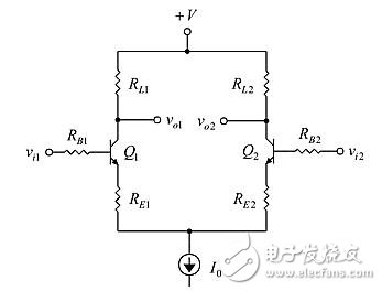
Figure 1: Differential Input Differential Output Voltage Amplifier.
This is a differential input differential output voltage amplifier. In the case of differential input and output, the incremental voltage gain of the circuit is:
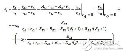
The condition for differential amplification is Aν1 = Aν2. When the circuit satisfies the following equation, it is symmetrical:

Then the voltage gain becomes:
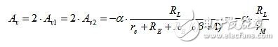
Where rM is a mutual resistance, and an output current generated by the input voltage (pre-α) flows through the resistor.
A good design goal is to make Aν a fixed value. One of the influencing factors is the choice of resistors with a low temperature coefficient (TC) and sufficiently accurate, which is usually easy to implement. However, for high-precision design, the change in resistance caused by changes in ambient temperature is a factor to consider. In particular, consider the "thermal effect", which is the dynamic, waveform-dependent resistance change caused by the change in power consumption as a function of νi. For very precise designs, the change in resistance associated with the applied voltage must also be considered.
In the exact design, in addition to the two (re and β) BJT T model parameters used here, Other transistor parameters, ie, ro, also need to be taken into account. We assume that the BJT has a sufficiently high Early voltage, so there is no need to consider the ro - at least not considered here. In practice, this assumption is usually valid.
BJT is usually the least desirable component in a circuit. As can be seen from the gain equation, the two BJT parameters of the incremental emitter resistances re and β affect the gain. For high beta values ​​- ie, beta >> 1, the gain factor is close to 1:

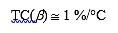
For a typical beta value of 200, α = 0.995, resulting in a gain error of 0.5%. If the difference is too large, an alpha compensation technique is required. Usually, this error can be compensated by including it in the gain formula, as we have done. More important is the size of its temperature drift. Typical values ​​are:
Then for large β, the TC of α is about 50 ppm; α is usually not a big problem.
Av's mutual resistance expression rM (denominator) is the resistance of the input voltage to produce the (emitter) current common to the input and output loops. The output current is modified by α, resulting in loss of the current path of the transmitter. The mutual resistance rM also includes β expressed in RB. If RB is kept at a small value and the input is driven by a voltage source, then β is not considered. If the resistance of the source is high, then the RB term will affect the gain due to the change in temperature with β. Its 1%/°C change is reduced to the extent that RB/(β + 1) is not dominant in rM. Keeping RB small is another design consideration factor.
The most troublesome item in rM is re because it varies with temperature and emitter current IE, according to:
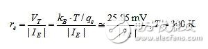
In the case where IE is constant, re varies with the thermal voltage VT, and VT varies in proportion to the absolute temperature.

At 300 K (about 80 °F), this value is 1/300 K or about 0.33 %/K = 0.33 %/°C. For laboratory-quality instrument design, we assume a temperature range of more than 25 ° C +/- 15 ° C, that is, 10 ° C to 40 ° C, beyond this range of equipment should be able to meet the normal operating conditions. In the case where the ambient temperature changes by more than 15 ° C, the VT changes by about 5%, which is too large for most precision designs. Therefore, it is necessary to compensate for the VT variation of the gain.
The simplest way to compensate for re is to treat it as a negligible item (along with the RB entry) in rM. This is achieved by making RE dominate. For RE>>re, the drift of re has a much lower effect on gain than 5%. In many cases, the dominant external emitter resistance solves the drift problem, but at the expense of gain and power. By increasing I0, re decreases proportionally, but the circuit power consumption increases. This is not only disadvantageous for power-constrained devices, but also exacerbates heat by increasing ΔPD(νi) in BJT.
In some cases, re can't be ignored, and some compensation is needed. One of the most common methods is to have I0 track re and offset its effects. In order for I0 to have a TC of VT, the easiest way is to implement I0 using a BJT current source. The be junction voltage of the current source BJT decreases with temperature rise, and I0 increases and re decreases.
Current source circuit
The first circuit source I0 we will consider is nothing more than a resistor R0, which returns to the negative supply. This "long tail" current source is close to the ideal current source when the supply voltage -V approaches negative infinity or the value of R0 approaches infinity. It does not compensate for the TC of re.
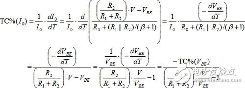
The implementation of the second consideration is shown below.
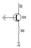
Figure 2: The voltage across the circuit at R0 is V – VBE(Q0).
The voltage of this simple circuit across R0 is V – VBE(Q0). As the temperature increases, the VBE decreases, but it is independent of the TC of VT. Another major BJT parameter affecting VBE is the saturation current IS found in the pn junction (be junction) voltage equation:
For a typical BJT (eg PN3904), IS ≈ 10 fA. Then, a current of 1 mA produces a VBE of 0.65 V.
Both VT and IS have an impact on TC (VBE). The effect of IS on VBE is greater than VT and the opposite polarity results in a total impact on VBE of approximately –2 mV/°C. Therefore, canceling the IS impact is more important than VT.
Depending on the relative values ​​of V and VBE, the effect of TC(VBE) can be adjusted by selecting RE and supply voltage V, which is typically limited by system level design. Thevenin equivalent supply voltage and R0 can be set independently by adding a resistor network between the emitter and ground. If adjusted correctly, as T increases, VBE decreases and I0 increases. If the decrease in re caused by increasing T cancels out the increase in re caused by VT, then the re and gain of the BJT pair remain unchanged.
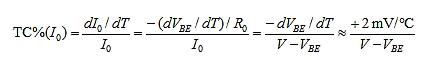
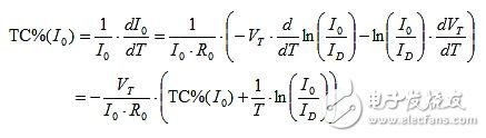
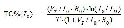
By using T to differentiate re, TC(re) is calculated as follows:

Where TC% is the fractional change of TC.
The setting of TC%(I0) = TC%(IE) can be constructed as follows. The only change on R0 comes from the VBE. Therefore, the fractional change in I0 caused by T is:
Set TC%(I0) = TC%(VT) = 1/T≅ 0.33 %/°C, the voltage across R0, V – VBE = 0.6 V. This compensation scheme is less attractive at -V = -1.25V. The polarity of TC(I0) is correct for compensation, but the amplitude is not required, so the next solution is shown in Figure 3.
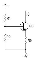
Figure 3: The polarity of TC(I0) is correct for compensation, but the amplitude is not required, so there is a new solution.
The implementation of I0 is more versatile and more common than previous solutions. The basic divider provides additional freedom to set TC%(I0), which helps to ignore TC(β), now:
The partial pressure ratio that provides the correct compensation can now be found. When TC%(I0) is set equal to TC%(VT), then:
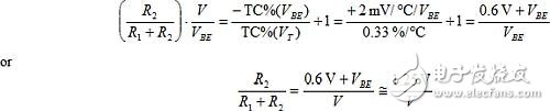
This result is very interesting; regardless of the V value, the no-load divider voltage must be 1.25 V for gain compensation. This is also the bandgap reference voltage and should be. The bandgap circuit uses a negative TC (VBE) and is adjusted to cancel the positive TC (VT). The resulting bandgap voltage is always close to 1.25V and varies slightly depending on the BJT doping level.
Another current source scheme often used to provide coarse temperature compensation is to insert a diode in series with R2, as shown in Figure 4.
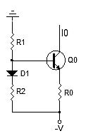
Figure 4: A current source scheme often used to provide coarse temperature compensation is to insert a diode in series with R2.
A common explanation is that the TC of the diode compensates for the TC of the BJT be junction, resulting in a more stable I0. A typical example is the use of a 1N4152 diode to compensate for the PN3904. However, the diode and the BJT be junction are completely different. In order to achieve a higher breakdown voltage, the doping level of the diode is much lower than that of the BJT base. In order to obtain good emitter-to-base injection efficiency, the emitter minority carrier concentration is intentionally increased, which is at the expense of VBE reverse breakdown. VBE reverse breakdown is usually around 7V, much lower than 40V of the diode. The key is that although both junctions are silicon, they are quite mismatched.
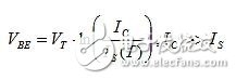
If a similar BJT be junction is assumed to be used as a diode and its base is connected to the collector, then the junction matching is much better (although not as good as the adjacent integrated BJT) and allows α ≅ 1 and then around the BJT input loop Apply Kirchhoff's voltage law (IS of two BJT junctions is eliminated):
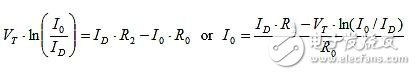
Where ID is the diode current. If the junction currents are equal, the TC of VT is removed and TC%(I0) ≅ 0 %/°C. This is useful for applications that require a stable current source, but it does not compensate for the re of the differential amplifier. In order to get the required TC, the current must be intentionally set to be unequal, and it must be positive for the compensated polarity of the TC. Therefore, we must have ID>I0.
TC%(I0) is obtained by the implicit function differential of I0 in the above formula:
Through another algebraic operation:
Then compensate, set TC%(I0) = TC%(VT) = 1/T, solve:
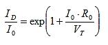
The actual current ratio requires that the voltage across R0 be not greater than VT due to the exponential function. For I0 = 2mA, R0 = 22Ω, VT = 26 mV, the voltage across R0 is 44mV or 1.69xVT, and ID = 14.77xI0 = 29.5mA, which is greater than what is required for most designs. In order for R0 to not dominate the transmit junction circuit, R0 is required to be such a small value that it can represent the TC of the VBE. However, in many designs, R0 is relatively large and its pressure drop is much higher than VT. Therefore, the TC% (VT) of re is not properly compensated, and there is a TC drift in the gain.
The previous scheme omits the base diode and is only slightly better in allowing a larger R0 voltage. Maybe we should go backwards and add one or two diodes to the emitter. The combined TC will be the single junction TC multiplied by the combined number, which will cause the RE to scale up. We usually do not want to add a large number of series diodes, as this will cause the static stability of I0 to deteriorate. Therefore, temperature compensation for re using a differential amplification current source requires careful circuit design. I0 is then made sensitive to the junction parameters, and these parameters (such as IS) have a slightly wider tolerance in discrete transistors, even with the same part number. For the PN3904BJT, products of different suppliers or production lots may have a difference of up to 50mV under the same current and temperature conditions. This compensation method is best suited for monolithic integration.
in conclusionIt is generally accepted that the BJT current source can compensate for temperature compensation of the BJT differential amplifier, but this is not universal. The temperature compensation of I0 for the constant re causes the voltage on the external emitter resistor R0 of the current source to become too low, so that I0 cannot be accurately set.
Therefore, in addition to the more complicated scheme of amplifying VT, in some designs, the RE dominant method for differential amplifier gain stability seems to be acceptable. Another solution with multiple stages is to use the continuous compensation (PNP) stage to eliminate the gain TC of the first stage.
Motorola Mobile Radio,Motorola Walkie Talkie Phone,Motorola Vhf Mobile Radio,Motorola P25 Mobile Radio
Guangzhou Etmy Technology Co., Ltd. , https://www.digitaltalkie.com