
Implement FFT algorithm with FFT IP Core
Abstract: In combination with engineering practice, a method of implementing FFT using FFT IP Core is introduced. The design can simultaneously perform 256-point FFT operation on two real-number sequences, and perform modulo square operation on the conversion result, and have continuous processing on the data. ability. The design adopts low-cost FPGA implementation, which has the characteristics of low cost, high performance, high flexibility, fast speed, etc., and it proves that the design is correct and feasible through engineering application.
Thanks to the advent of FFT (Fast Fourier Transform), the discipline of digital signal processing has been promoted, and it can be applied to any field that can be applied to Fourier transform theory. The traditional implementation of FFT is nothing more than software (software programming) and hardware (dedicated chip ASIC). The emergence of FPGA has made people have another choice in the implementation of FFT. FPGAs combine the flexibility of software programming with the speed of ASIC circuits for high-speed digital signal processing. Most FPGA vendors offer configurable logic cores to implement various algorithmic functions, including the FFT IP Core. Using these resources allows designers to spend more time and effort on improving system functionality, which will undoubtedly reduce design risk and shorten development cycles.
This design adopts Altera's FFT IP Core to realize FFT function. It can realize FFT conversion of two 256-point real data at the same time, and perform modulo square operation on the conversion result, and design the ability to continuously process data. The FPGA chip selects the lowest cost Altera Cyclone series chip. The FFT core is Altera MegaCore FFT-V2.0.0. The whole design cost is low and the performance is good. It has been successfully applied to radar products.
2 Algorithm principle and FFT Core introduction The algorithm used in the design includes FFT algorithm and CORDIC algorithm which simultaneously calculate two real functions.
2.1 FFT algorithm for simultaneously calculating two real functions DFT (Discrete Fourier Transform) is defined as: ![]()
In equation (1), it is assumed that the time function x(n) is a complex function. But in many practical applications of FFT, the time function is often a real function. The algorithm described below can effectively reduce the computational workload of real-order FFTs, thereby increasing the computational speed. This method can be summarized into the following steps:
1 function h(n) and g(n) are two real functions, n=0,1,...,N-1;
2 Take one of them as the real part and the other as the imaginary part, and form the complex function z(n) as:
z(n)=h(n)+jg(n), n=0,1,...,N-1;
3 Calculate the N-point DFT of z(n): ![]()
Where Zr(k) and Zi(k) are the real and imaginary parts of Z(k), respectively;
4 Analyze H(k) and G(k) from z(k): 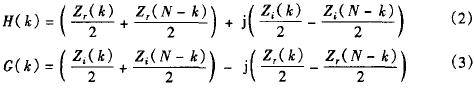
Where H(k) and G(k) are the DFTs of h(n) and g(n), respectively.
The detailed derivation process is described in the literature [2].
2.2 CORDIC algorithm principle The CORDIC (The Coordinate RotaTIonal Digital Computer) algorithm is a loop iterative algorithm whose basic idea is to approximate the angle of rotation required by a series of constant yaw angles related to the operating base. In a broad sense, it is a numerical method of approximation. Since these fixed angles are related to the calculation of the base, the operation is only shifted and added. Functions that can be calculated using this algorithm include multiplication, division, square root, sine, cosine tangent, vector rotation (ie, complex multiplication), and exponential operations. The basic principles of CORDIC are as follows.
The vector x+jy, the rotation angle θ to the vector x'+jy', the assumed direction is represented by δ, the angle of rotation is θi, and θi satisfies the relationship: tan θi=2i. From the derivation of the literature [3], we can see: 
Assuming x[0]=b, y[0]=a,z[0]=0, then: ![]()
In the formula, ![]() For the distortion factor, for a certain operation of the word length, it is a constant, such as when the word length is 16 bits, K = 1.6667. Δi represents the direction of each rotation, when y[i] ≥ 0, its value is 1; when y[i] ≤ 0, its value is -1.
For the distortion factor, for a certain operation of the word length, it is a constant, such as when the word length is 16 bits, K = 1.6667. Δi represents the direction of each rotation, when y[i] ≥ 0, its value is 1; when y[i] ≤ 0, its value is -1.
2.3 Introduction to FFT Core FFT-V2.0.0 is a new FFT intellectual property core released by Altera in February 2004. It is a high performance, highly parameterized Fast Fourier Transform (FFT) processor supporting Cyclone.
StraTIx II, StraTIx GX, and StraTIx family of FPGA devices. The FFT Core function performs a high performance forward complex FFT or inverse FFT (IFFT) using a base 2/4 frequency domain decimation (DIF) FFT algorithm with a conversion length of 2 m, where 6 ≤ m ≤ 14. Internally, the FFT uses a block floating-point structure to maximize the gain between maximum signal-to-noise ratio (SNR) and minimum resource requirements. The FFT Core receives a complex-length sequence of length N, two's complement format, and sequential input as input, and outputs a sequence of complex data sequences of the conversion domain. At the same time, an accumulated block index is output, indicating the quantization factor of the block floating point. The conversion direction of the FFT Core is previously specified by an input port for each data conversion block.
The FFT Core can be configured with two different engine architectures: a Quad-output FFT engine and a Single-output FFT engine. For applications that require as little conversion time as possible, a four-output engine architecture is the best choice; for applications that require as few resources as possible, a single-output engine architecture is appropriate. To increase the throughput of the entire FFT Core, a multi-parallel engine architecture can be employed.
The FFT Core supports three I/O data stream structures: streaming, Buffered Burst, Burst. The continuous I/O data stream structure allows continuous input data to be processed and outputs continuous complex data streams without interrupting input and output data; buffered burst I/O data stream structures require less storage resources than continuous structures, but This is at the expense of reducing the average throughput; the operation of the burst data stream structure is basically the same as the buffer burst mode, but the burst mode requires less storage resources, which is also at the expense of lowering the throughput.
3 hardware design 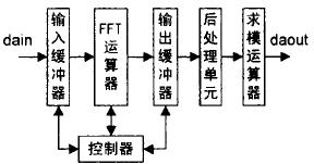
Figure 1 overall schematic diagram The overall schematic of the design is shown in Figure 1. The input and output buffers store the preprocessed data and the FFT conversion result respectively; the FFT operator is responsible for the FFT operation; the controller provides the read and write addresses for the input and output buffers, and controls the timing of the FFT operation and the read and write operations of the buffer; The processing unit separates two real input spectral data from the single-pass complex input spectral data; the modulo operator implements the CORDIC algorithm to obtain the square root of the conversion result. The input of the design is two real-number sequences, one as the real part and the other as the imaginary part, consisting of 256 consecutive data segments; the output is a discontinuous 256-point data segment, and the first 128 points of each data segment are the first The spectrum data, the last 128 points is the second channel spectrum data. According to the symmetry result of the FFT spectrum with respect to the center point, only the first half of the spectrum data is intercepted without losing any information.
The working sequence of the entire system is:
1 data is input to the input buffer at a rate of 5 MHz;
The 2 FFT operator operates on the input buffer at a rate of 40 MHz;
At the end of the 3FFT operation, the conversion result is stored in the output buffer;
4 output buffer data is sent to the post-processing unit for conversion at a rate of 20 MHz;
5 data is sent to the modulo operator, CORDIC operation, output;
6 When the end of 3, the FFT operator returns to the initial state, waiting to process the next set of data, so that the operation is repeated. The entire design is strictly controlled by the controller.
The input and output buffers are implemented by the internal RAM of the FPGA, which are relatively simple. The following highlights. FFT operator, controller, post-processing unit, and modulo operator.
3.1 FFT operator The FFT operator is implemented by FFT Core. The engine structure is dual-single-output, and the I/O data stream is in burst mode. The FFT Core uses the Atlantic Interface protocol, the input interface is considered the primary receiver, and the output interface is considered the primary transmitter. The specific interface definitions are shown in Table 1.
| signal | direction | description |
| Clk | enter | FFT system clock signal |
| Reset | enter | FFT high effective synchronous reset signal |
| Master_sink_dav | enter | Master receiver data valid signal |
| Master_sink_ena | Output | Master receiver write enable signal |
| Master_sink_sop | enter | Input packet start bit indication signal |
| Inv_i | enter | Conversion direction control signal |
| Date_real_in[M-1...0] | enter | Enter real data |
| Data_imag_in[M-1...0] | enter | Enter imaginary data |
| Fft_real_out[M-1...0] | Output | Output real data |
| Fft_imag_out[M-1...0] | Output | Output imaginary data |
| Exponent_out[5...0] | Output | Signed data block index |
| Master_source_dav | enter | Sub receiver receives valid indication signal |
| Master_source_cna | Output | Master transmitter enable signal |
| Master_source_sop | Output | Output packet start bit |
| Master_source_eop | Output | Output packet end bit |
The specific workflow: after the system reset, the data source sets master_sink_dav to indicate that there is sampled data waiting for input; in response, the FFT Core sets master_sink_ena to indicate that it can receive input data; the data source loads the first complex data, and master_sink_sop Set to indicate the start of the input data block; the next clock, master_sink_sop is cleared, and the input data is added in natural order. When the input data reaches 256 points, the system naturally starts the FFT operation. The FFT conversion direction of a single data block can be changed by setting/clearing the inv_i signal. The inv_i signal must be strictly synchronized with the master_sink_sop signal. When the FFT conversion ends, the sub-receiver has set the master_source_dav signal, indicating that the sub-receiver can receive the conversion result of the FFT; at the same time, the master_source_ena signal is set, and the FFTCore outputs the operation result in natural order; during the output process,
The master_source_sop and master_source_eop signals are asserted to indicate the start and end of the output data block. See the literature [4] for a detailed description.
3.2 Controller and Post-Processing Unit The controller can be roughly divided into three parts: input buffer control (c_i), FFT operation control (c_f), and output buffer control (c_o). C_i provides read/write address and corresponding read/write control signals for the input buffer; c_f provides control signals for the FFT operator to strictly control the timing of the FFT Core; c_o provides read/write addresses and read/write for the output buffer control signal. The controller can be easily implemented by the state machine method of VHDL language programming.
The post-processing unit is actually a hardware implementation of equations (2) and (3). The specific principle is shown in Figure 2. 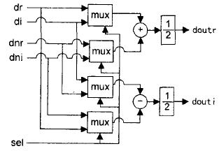
Figure 2 Schematic diagram of the post-processing unit schematic diagram "mux", "+", "-", "1/2" respectively represent the selector, adder, subtractor and divider, dr, di, dnr, dni and Zr(k) in formula (1) and formula (2),
Zi(k), Zr(Nk), and Zi(Nk) correspond. When sel is equal to 0, the spectrum data G(k) of the first real sequence is extracted to implement the function of equation (1); when sel is equal to 1, the spectrum data of the second real sequence is extracted to implement the function of equation (2).
3.3 Molding Operator Since the project only requires the square root and does not involve the calculation of the angle, the angle calculation part of CORDIC is not given, but this does not affect the calculation of the amplitude. The entire CORDIC adopts a full-pipeline structure, and the design has a total of 16 stages of pipeline units, and the structure of each pipeline unit is similar. The CORDIC pipeline structure is shown in Figure 3. 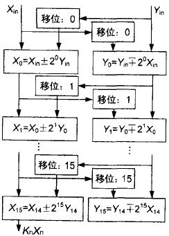
Figure 3 CORDIC Pipeline Schematic The result is not the final result, plus a magnitude correction to remove the effects of the distortion factor.
4 Conclusion The design of the input and output operating frequency is relatively low, so it is easy to meet, the key is the performance index of the FFT Core. According to the engineering needs, the input data rate is 5MHz, the FFT Core works at 40MHz, and the output conversion result is 20MHz clock. Under this condition, the design is hardware tested. The result proves that the design function is correct, the work is stable, and the performance is superior. In addition, the software timing simulation shows that the FFT Core's maximum operating frequency can reach 117.52MHz, and by increasing the operating clock, it can also get faster computing power.
The design uses Altera's FFT Core, and successfully implements two continuous 256-point real-sequence FFT algorithms in FPGA. Its design cost is low and its performance is good. It has been successfully applied to radar products. Due to the flexibility of the FFT Core, the design can be easily adapted to different products by changing the parameter settings.
references
[1] Uwe Meyer-Baese. FPGA implementation of digital signal processing [M]. Beijing: Tsinghua University Press, 2003.
[2] Hou Zhaohuan, Ru Shizun, Jiang Yinlin. Practical FFT Signal Processing Technology [M]. Beijing: Ocean Press, 1990.
[3] Tan Yiyu, Yan Wenbing, Li Yuan et al. An R-θ Transform ASIC Based on CORDIC Algorithm[J].Microelectronics,2000,30(3):166~167.
[4] Li Wei, Han Yueqiu. Trigonometric Function Generator Based on Pipeline CORDIC Algorithm. System Engineering and Electronic Technology [J], 2000, 22(4): 85-87.
LED - Angel Eyes Marker,Certified Angel Eyes Marker,Quality Angel LED Eyes Marker,LED Angel Eyes Head Lamp
LED Headlight LED Fog Light Co., Ltd. , http://www.nbledheadlight.com