
introduction
In switching power supplies, EMI filters play a significant role in suppressing common mode and differential mode conducted noise. Based on the study of the filter principle, a method for independent analysis and separate modeling of common mode and differential mode signals is discussed. Finally, a design procedure of EMI filter is proposed based on this.
High-frequency switching power supplies have been widely used in various fields such as industry, national defense, and home appliances due to their many advantages in terms of volume, weight, power density, and efficiency. In the case where the switching power supply is applied to the AC grid, the rectifier circuit often causes the input current to be discontinuous, which not only greatly reduces the input power factor, but also adds a large number of higher harmonics. At the same time, the high-speed switching action of the power switch tube in the switching power supply (from tens of kHz to several MHz) forms an EMI (electromagnetic interference) disturbance source. According to the published research on switching power supply, the main forms of interference in switching power supply are conducted interference and near-field radiation interference. Conducted interference will also be injected into the power grid and interfere with other equipment connected to the power grid.
There are many ways to reduce conducted interference, such as laying a ground wire reasonably, adopting star-shaped paving, avoiding a circular ground wire, minimizing common impedance, designing a reasonable buffer circuit, and reducing circuit stray capacitance. In addition, EMI filters can be used to attenuate noise interference between the grid and the switching power supply.
EMI disturbances are often difficult to describe accurately. Filters are usually designed by iterative iterations and computational production to gradually approach the design requirements. This paper starts with the principle of EMI filtering, and gives the method of designing the filter in actual work by analyzing the common mode and differential mode noise model respectively, and gives the design example in steps.
1, EMI filter design principle
In the switching power supply, the main source of EMI disturbance is the dv/dt and di/dt generated by the switching action of the power semiconductor device. Therefore, the electromagnetic emission EME (Electromagnetic Emission) is usually a broadband noise signal, and its frequency range is from the switching operating frequency to several. MHz. Therefore, the measurement of the conducted electromagnetic environment (EME), as specified by many international and national standards, ranges from 0.15 to 30 MHz. Designing an EMI filter is to give sufficient attenuation to the switching frequency and the noise of its higher harmonics. Based on the above criteria, it is usually considered to attenuate the EME with a frequency higher than 150 kHz to a reasonable range.
The low-pass filter concept generally accepted in the field of digital signal processing is equally applicable to power electronic devices. In short, the EMI filter design can be understood to meet the following requirements:
1) The required stopband frequency and stopband attenuation; (the attenuation of Hstop is required to meet a certain frequency fstop);
2) low attenuation of the grid frequency (satisfying the specified passband frequency and low attenuation of the passband);
3) Low cost.
1.1, commonly used low-pass filter model
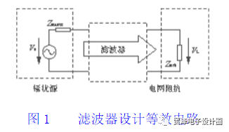
The EMI filter is usually placed at the front end of the switching power supply connected to the grid. It is a low-pass filter consisting of a series reactor and a shunt capacitor. As shown in Figure 1, the equivalent impedance of the noise source is Zsource, and the equivalent impedance of the grid is Zsink. The filter indices (fstop and Hstop) can be implemented by first-order, second-order or third-order low-pass filters. The calculation of the filter transfer function is usually approximated at high frequencies, that is, for n-order filters, all ωk correlations are ignored. The term (when k) only takes the ωn related term. Table 1 lists several common filter topologies and their transfer functions. Special attention should be paid to the effects of input and output impedance mismatch on the filter characteristics.

1.2, EMI filter equivalent circuit
Conducted EMI noise includes both common mode (CM) noise and differential mode (DM) noise. Common mode noise exists between all AC phase lines (L, N) and common mode ground (E). The source of the noise is considered to be the insulation leakage current between the two electrical circuits and the electromagnetic field coupling; the differential mode noise exists in the AC phase. Between the lines (L, N), the source of the ripple current, the ringing current of the switching device, and the reverse recovery characteristics of the diode. The two modes have different sources of conducted noise and different conduction paths, so the common mode filter and the differential mode filter should be designed separately.
Obviously, it is necessary to separate the two different modes of conducted noise and measure the actual level separately, which will help to determine the noise of that mode and the corresponding part of the filter design process. In the implementation of parameter optimization.
Taking a common filter topology (Fig. 2(a)) as an example, the equivalent circuits of common mode and differential mode noise filters are analyzed. Figure 2(b) and Figure 2(c) represent the filter common mode attenuation and differential mode attenuation equivalent circuit, respectively. The analysis circuit shows that Cx1 and Cx2 are only used to suppress differential mode noise, and the ideal common mode choke inductor LC is only used to suppress common mode noise. However, due to the asymmetry of the actual LC winding, the presence of a leakage inductance Lg between the two sets of LCs can also be used to suppress differential mode noise. Cy can suppress common mode interference and suppress differential mode noise, but since the differential mode suppression capacitor Cx2 is much larger than Cy, Cy can negligible differential mode suppression. Similarly, LD can suppress both common mode interference and differential mode interference, but LD is much smaller than LC, so the suppression of common mode noise is relatively small.
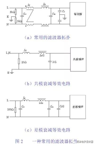
It can be deduced from Table 1 and Figure 2. For the common mode equivalent circuit, the filter model is a second-order LC type low-pass filter, the equivalent common mode inductance is recorded as LCM, and the equivalent common mode capacitance is recorded as CCM. Have
LCM=LC+1/2LD(1)CCM=2Cy(2)
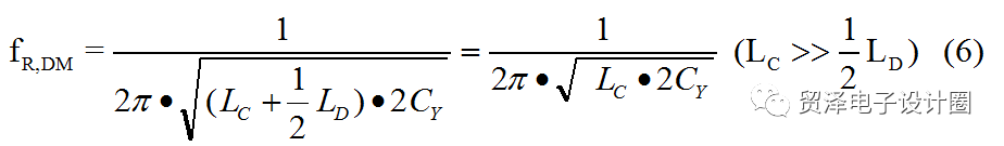
For the differential mode equivalent circuit, the filter model is a third-order CLC type low-pass filter, the equivalent differential mode inductance is recorded as LDM, and the equivalent differential mode capacitance is recorded as CDM (so that Cx1=Cx2 and Cy/2< ), then there is
L=2LD+Lg(3)
CDM=Cx1=Cx2(4)
The LC filter cutoff frequency is calculated as
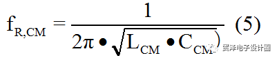
Substituting equations (1) and (2) into equation (5), there is
The CLC type filter cutoff frequency is calculated as
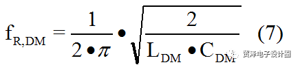
Substituting equations (3) and (4) into equation (7), there is

In the case where the noise source impedance and the grid impedance are both determined and matched, the EMI filter suppresses the common mode and differential mode noise, as shown in FIG.
2, the actual method of designing EMI filters
2.1, some considerations in the design
The effect of the EMI filter depends not only on itself, but also on the noise source impedance and the grid impedance. The grid impedance Zsink is usually calibrated using a static impedance compensation network (LISN), connected between the filter and the grid, including the inductor, capacitor and a 50 Ω resistor to ensure that the grid impedance can be determined from known standards. The EMI source impedance depends on the different converter topology.
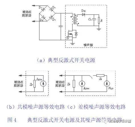
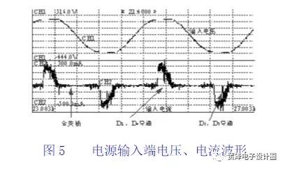
Taking a typical flyback switching power supply as an example, as shown in Fig. 4(a), the current of the full bridge rectifier circuit is intermittent, and the current and voltage waveforms are as shown in Fig. 5. For common mode noise, Zsource shown in Figure 4(b) can be viewed as a current source IS in parallel with a high impedance ZP; in Figure 4(c), for differential mode noise, depending on the rectifier bridge diode on and off, Zsource has two State: When any two of the diodes are turned on, Zsource is equivalent to a voltage source VS connected in series with a low-value impedance ZS; when the diode is all turned off, it is equivalent to a current source IS and a high-impedance ZP in parallel. Therefore, the noise source differential mode equivalent impedance Zsource is switched between the above two states at twice the power frequency.
In the aforementioned design process, EMI filter components (inductance, capacitance) are considered to be ideal. However, due to the parasitic parameters of the actual components, such as the parasitic inductance of the capacitor, the parasitic capacitance between the inductors, and the parasitic parameters of the PCB layout, the actual high-frequency characteristics are often quite different from the ideal component simulation. This involves many problems such as EMC high-frequency modeling. The parameters of the model are often difficult to determine. Therefore, this paper only considers the low-frequency suppression characteristics of the EMI filter. Therefore, the values ​​of ZS and ZP are related to the parasitic parameters such as parasitic capacitance, inductance and equivalent capacitance of the rectifier bridge. It is difficult to directly solve the source impedance according to the circuit topology and parameter modeling scheme. Therefore, the actual measurement Zsource is often used in the design. .
2.2, the actual design steps
EMI filter design often requires that the volume be as small as possible and the cost should be as low as possible while achieving noise suppression. At the same time, the filtering effect also depends on the actual noise level. The interference weights of common mode and differential mode noise are analyzed. To this end, the following parameters are required to be determined before design to achieve design optimization.
1) Measure the equivalent impedance Zsource of the interference source and the equivalent impedance of the grid. In the actual process, it is often guided by theory and experience. The PCB board of the power supply is first made. This is because the noise source and the interference path of the common mode and differential mode are different from each other. The slight difference in the trace of the circuit board may lead to a large EME. Variety.
2) Measure the interference noise spectrum before adding the filter, and use the noise separator to separate the common mode noise VMEASUREE, CM and the differential mode noise Vmeasure, CM to make the corresponding interference spectrum.
Then the actual design can be carried out. Still taking the filter model proposed in this paper as an example, the steps are as follows.
(1) Calculate the common mode and differential mode attenuation required by the filter according to equation (9), and make curves Vmeasure, CM-f and Vmeasure, DM-f, where Vmeasure, CM and Vmeasure, DM have been measured, Vstandard , CM and Vstandard, DM can be set with reference to the national standard for conducted EMI interference. The reason for adding 3dB is that the measured value of the noise separator is 3 dB larger than the actual value.
(Vreq, CM) dB=(Vmeasure,CM)-(Vstandard,CM)+3dB
(Vreq, DM) dB=(Vmeasure,DM)-(Vstandard,DM)+3dB(9)
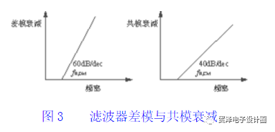
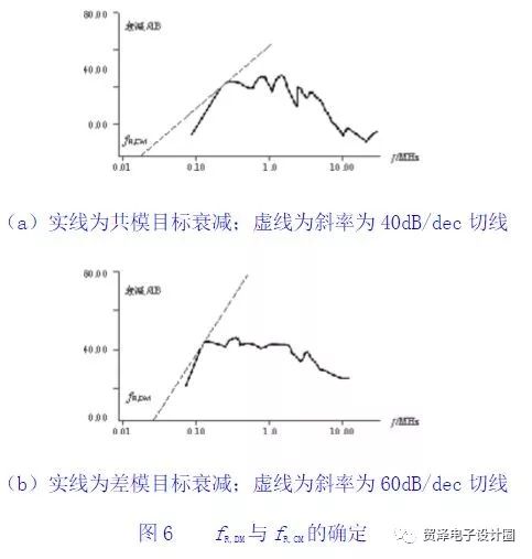
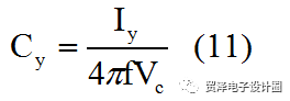
(2) As can be seen from Fig. 3, the intersection of the two oblique lines with the slopes of 40 dB/dec and 60 dB/dec, respectively, is fR, CM and fR, DM. For Vmeasure, CM-f and Vmeasure, the tangent of DM-f, the tangent slopes are 40dB/dec and 60dB/dec, respectively. As you can see, by measuring their intersection with the frequency axis, you can get fR, CM and fR, DM. Figure 6 shows its schematic diagram.
(3) Filter component parameter design
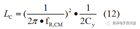
——The selection of common mode parameters Cy is connected between the phase line and the earth. If the capacity of the capacitor is too large, the leakage current will be too large and the safety will be reduced. The smaller the leakage current requirement, the better. The safety standard is usually several hundred μA to several mA.
The calculation formula of EMI to ground leakage current Iy is
Iy=2Ï€fCVc(10)
Where: f is the grid frequency.
In this example, Vc is the voltage drop across capacitor Cy, f = 50 Hz, C = 2Cy, Vc = 220/2 = 110V, then
If the ground leakage current is set to 0.15 mA, Cy ≈ 2200 pF can be obtained. Substituting Cy into step (2) to obtain fR, CM value, and then fR, CM into equation (6)
——The selection of differential mode parameters is known from equation (8). There is no unique solution for the selection of Cx1, Cx2, and LD, which allows the designer to have a certain degree of freedom.
As can be seen from FIG. 2, the leakage inductance Lg of the common mode inductor Lc can also suppress differential mode noise, and the LD can be omitted in order to simplify the filter. Experience has shown that the leakage inductance Lg is mostly 0.5% to 2% of the Lc value. Lg can be obtained by measurement. At this time, the values ​​of Cx1 and Ccx2 are correspondingly larger.
3, the conclusion
The discussion in this paper is based on low-frequency model analysis of low-pass filters. Due to the influence of the actual component parasitic parameters, especially in the high frequency band, it is often necessary to repeatedly correct the parameters after the first parameter determination, and to use the low ESR and ESL capacitors to optimize the material and process of the wound core, and gradually approach Required technical indicators.
Since only a single-stage filter design is involved, such as LC-type filter attenuation is only 40dB/dec, when an attenuation degree of 60-80dB or more is required, a multi-stage filter is often required.
General-purpose EMI filters are often difficult to design. This is due to the fact that the electromagnetic environment levels vary greatly between different power converters due to topology, component selection, PCB layout, etc., plus the problem of impedance matching. The versatility of the filter is greatly affected. Therefore, the design of the filter often needs to be targeted and gradually corrected in actual debugging.
Capacitor Leakage Test Power Supplies
The ADP series capacitor leakage test power supply is specially designed and customized for capacitor manufacturers` product quality control process or users of capacitors for capacitor ripple current durability life test.

Capacitor leakage current test power supply is aimed at the diversity of output voltage and frequency required for different capacitance tests with the DC output voltage up to 3000Vdc, the AC voltage output up to 200Vac, the AC current up to 500A, and the output frequency can be selected according to customer requirements from 50Hz to 100KHz.
Equipped with special high-frequency and high-temperature fixtures and connecting wires for capacitor leakage current testing, the capacitor leakage current test power supply can imitate the actual working conditions of capacitors to determine the service life of a group of capacitors under test, providing the accurate parameters of capacitors required by the manufacturer for the capacitors R&D and quality inspection test, the power supply is now aiding the test of high-frequency and high-current passive devices such as high-frequency capacitors, film capacitors, electrolytic capacitors, ballast capacitors, and ballast inductors.
Capacitor Leakage Current Power Supplies, Leakage Current Ripple Power Supplies, AC and DC Power Supplies, Capacitor Test Power Supplies, Ripple Current Test Power Supplies
Yangzhou IdealTek Electronics Co., Ltd. , https://www.idealtekpower.com