
introduction
With the rapid development of information technology and integrated circuits, electronic products are gradually developing towards intelligence, miniaturization, and low power consumption. At the same time, the power supply must be small in size, high efficiency, and low power consumption to adapt to the rapid development of electronic products. Therefore, highly integrated PWM controllers are widely used in electronic products.
The step-down PWM controller APl510 launched by AnachiD Electronics can be widely used in the power supply of electronic products. Because the APl510 chip contains reference voltage source, oscillation circuit, error amplifier, internal PMOS switch tube and other circuits, only a small number of components such as inductors, capacitors and diodes are needed to form a small, high-efficiency step-down switch. Voltage power supply.
l APl5lO working principle
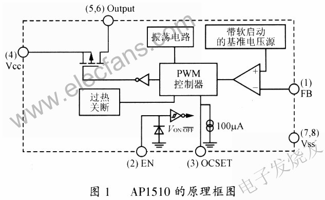
The functional block diagram of APl510 is shown in Figure 1.
1.1 Pin function and description
Pin 1 (FB) feedback terminal, the inverting input of the error amplifier, is connected to the power output terminal through the voltage divider resistor.
Pin 2 (EN) enable terminal, work or standby control, high level: normal operation, low level: standby operation.
Pin 3 (OCSET) output current setting terminal, the maximum output current is set by an external resistor.
Pin 4 (VCC IC) power input positive terminal.
Pins 5 and 6 (Output) switch output terminal, P-channel MOS field effect transistor drain, connect external freewheeling diode and inductor.
Pin 7, 8 (VSS IC) power input negative terminal.
1.2 Working principle
As can be seen from Figure 1, APl510 is composed of reference voltage source, oscillation circuit, error amplifier, PWM controller, thermal shutdown control circuit and P-channel MOS field effect transistor.
The reference voltage source provides a stable power supply voltage for the internal circuit of the chip, and a 0.8V voltage reference for the non-inverting input terminal of the error amplifier. It has a soft start function, which can prevent the impact when the power is started. It also has an undervoltage lockout function. When the input voltage is lower than 3.3V, the APl510 stops working; when the input voltage is higher than 3.5V, it automatically resumes work.
The oscillation circuit generates an oscillation waveform of 300 kHz. When overcurrent protection or short-circuit protection occurs, the operating frequency will be reduced from 300 kHz to 30 kHz.
The sampled signal of the output voltage enters the inverting input terminal of the error amplifier, enters the PWM controller after comparison, and outputs the square wave of the duty cycle change to drive the internal P-channel M0S tube: the duty of the APl510 adjustment pulse can be from 0% ~ 100%, which makes APl510 can work normally in a wide input voltage range.
The overheat shutdown circuit shuts down the chip when the junction temperature reaches 125 ° C, protecting the chip from damage due to overheating. The recovery temperature is 100 ℃, and the temperature difference of 25 ℃ ensures that the chip will not oscillate when it is overheated.
APl510 has the current limiting function of P-channel MOS tube, and its calculation method is
In the formula: ILOAD is the working current set by the internal P-channel MOS tube, and the maximum working current of the MOS tube in APl51O is 3 A;
RDS (ON) is the on-resistance of the MOS tube in APl510, and its value is 100mΩ;
IOCSET is the working current of the internal constant current source in APl5lO, its value is 100μA;
ROCSET is the external resistance of the pin OCSER to ground.
The input voltage range of APl510 is 3.6 ~ 23V, because of the built-in P-channel MOS tube, so only need to add an inductor, capacitor, diode, etc., can form a step-down switching regulator power supply. Due to the fixed frequency operation, the internal compensation circuit is simple, the output ripple is low, the transient response is good, and the efficiency of the power supply is also very high.
2 Application circuit
The circuit shown in Figure 2 is a typical step-down DC / DC converter composed of APl510, whose input voltage is 12 V and output voltage is 5V.
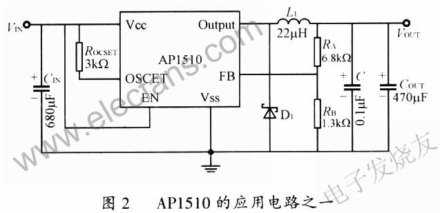
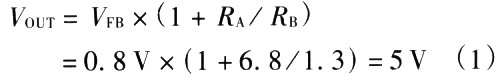
In the circuit of Fig. 2, RA and RB are the output voltage setting resistors, and the relationship between the output voltage VOUT and the resistance of RA and RB is listed in equation (1).
ROCSET is the maximum current setting resistance of the MOS tube, the maximum current of the M0S tube, and the relationship between IMOS and ROCET is listed in equation (2).
In the type: RMOS is the on-resistance of MOS tube, when VIN = 12V, the typical value of RMOS is 100mΩ.
For the occasions where the voltage regulation rate is high, the circuit shown in Figure 2 may not meet the requirements, while the circuit shown in Figure 3 not only has the voltage regulation rate compensation function, but also has a standby function. It can be directly controlled by the level of the CPU or other digital circuits, and can switch between "work / standby" modes without the need for additional interface circuits.
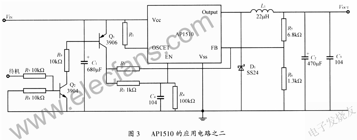
Figure 3 becomes the compensation resistor. The higher the input voltage, the stronger the feedback, and it acts as a voltage compensation; Q1 and Q2 are used for "on / standby" control, and at the same time, they cut off the compensation during standby. In actual application process, the size of R2 can be determined according to the input voltage range, especially when the input voltage is low (such as 6 ~ 12V), the effect is significant, and the input voltage is high (such as 12-20V) can be omitted.
3 Test results
According to the circuit shown in Figure 2, a 5 V output voltage regulator is designed and debugged. The test results are as follows.
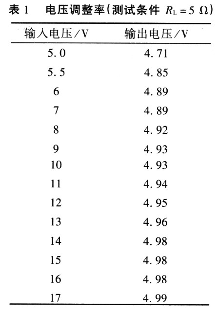
1) The voltage regulation rate is listed in Table 1.
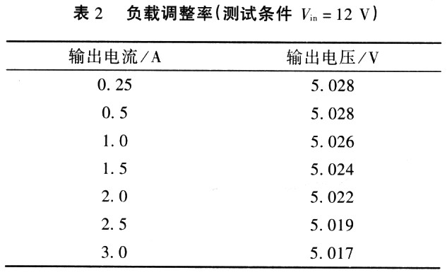
2) The load adjustment rate is listed in Table 2.
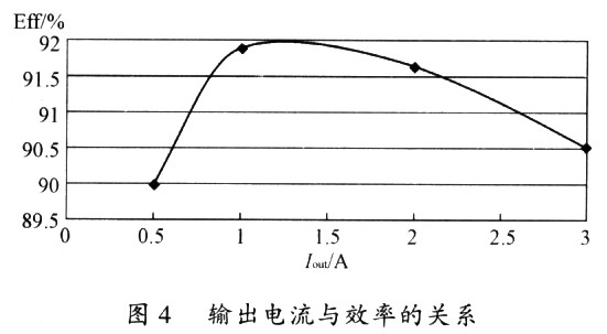
3) The relationship between output current and efficiency is shown in Figure 4.
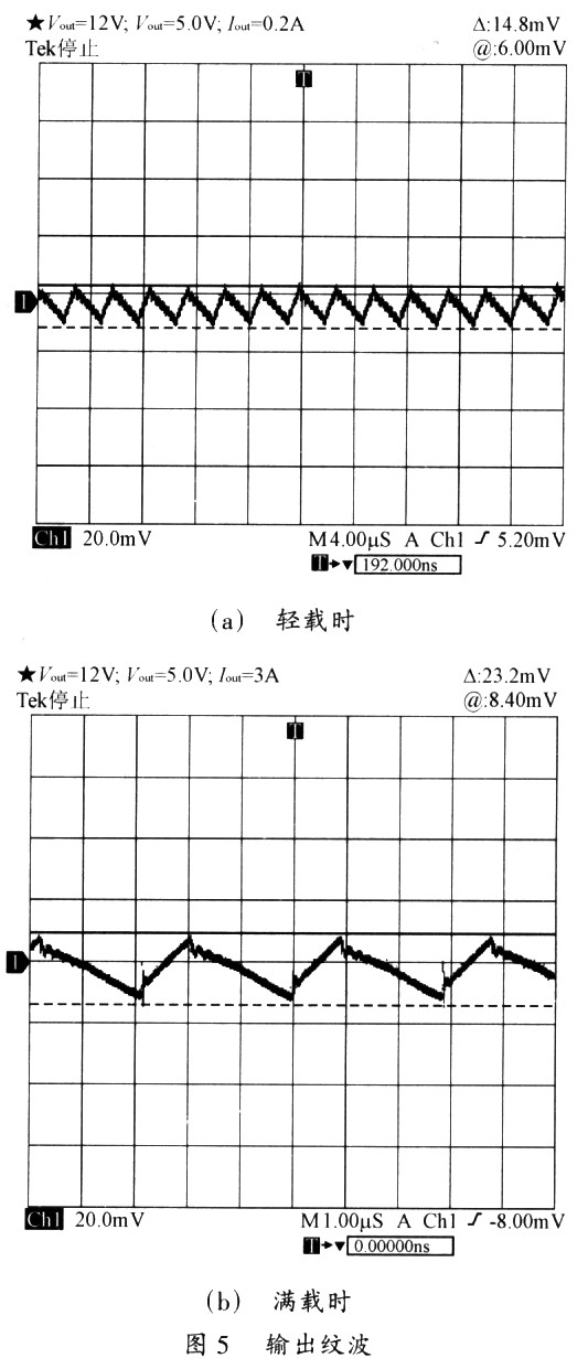
4) The output ripple is shown in Figure 5.
5) The relationship between input voltage and duty cycle is shown in Figure 6.
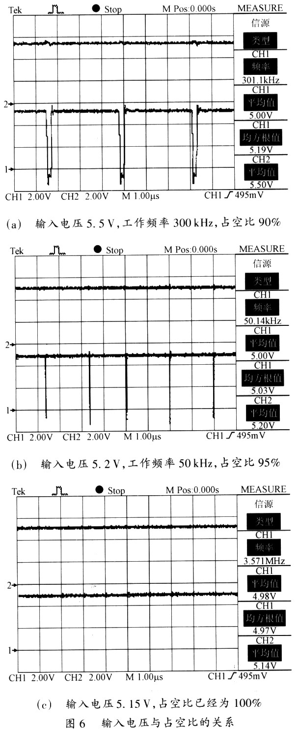
Test condition, load resistance: 5Ω. CHl is the output voltage waveform of 0utput pin, CH2 is the input voltage waveform, and the range is 2.OOV / div. In Figure 6 (a), the input voltage is 5.50V, the operating frequency is 300 kHz, and the duty cycle is about 90%. In Figure 6 (b), the input voltage is 5.20V, the operating frequency has been reduced to 50kHz, and the duty cycle is further increased, with a duty cycle of about 95%. In Figure 6 (c), the input voltage is 5.15V, the duty cycle width is already 100%, and the switch tube is in the through state.
Because the duty ratio of APl510 can reach 100%, VOET = 4 85V when VIN = 5.5V, and VOUT = 4.89 V when VIN = 6V, which is difficult for general PWM controller. Although APl510 has many advantages, but its voltage regulation rate is typically 1%. From the voltage adjustment data, especially in the case of lower input voltage, APl510 voltage adjustment rate is not too high.
4 Conclusion
The step-down PWM controller APl510 is highly integrated, the internal P-channel MOS tube has a small on-resistance, and the duty cycle can reach 100%. The step-down regulator composed of it has a simple circuit and high efficiency, so it is used in electronic products. The power supply has a wide range of applications.
The multimedia wiring harness apply to Audio,Video,Radio, LVDs,Flat RCA,USB.
Yacenter has experienced QC to check the products in each process, from developing samples to bulk, to make sure the best quality of goods. Timely communication with customers is so important during our cooperation.
If you can't find the exact product you need in the pictures,please don't go away.Just contact me freely or send your sample and drawing to us.We will reply you as soon as possible.
Electric Fan Wiring Kit,Socket Fan Wiring Harness,Custom Pc Wiring Harness,Multimedia Wiring Harness
Dongguan YAC Electric Co,. LTD. , https://www.yacentercns.com