
The input or front-end design of any high-performance ADC, especially an RF sampling ADC, is critical to achieving the required system-level performance. In many cases, the RF sampling ADC can digitally quantize the signal bandwidth of several hundred MHz. The front end can be active (using an amplifier) ​​or passive (using a transformer or balun), depending on the system requirements. In either case, components must be carefully selected in order to achieve optimal ADC performance in the target frequency band.
IntroductionThe RF sampling ADC is manufactured using deep sub-micron CMOS process technology, and the physical characteristics of the semiconductor device indicate that the maximum voltage supported by the smaller transistor size is also lower. Therefore, the absolute maximum voltage that should not be exceeded for reliability reasons specified in the data sheet, compared with the current mainstream RF sampling ADC compared with the previous old device, can be found that this voltage value is smaller.
In receiver applications that use ADCs to digitally quantize the input signal, system designers must pay close attention to the absolute maximum input voltage. This parameter directly affects the service life and reliability of the ADC. An unreliable ADC may render the entire radio system unusable, and the replacement cost may be huge.
To counteract the risk of overvoltage, the RF sampling ADC integrates a circuit that can detect high-level thresholds, allowing the receiver to compensate by adjusting the gain through an automatic gain control (AGC) loop. However, if a pipelined ADC is used, the inherent delay associated with the architecture may cause the input to be exposed to high levels, which may damage the ADC input. This article discusses a simple method to enhance the AGC loop and protect the ADC.
Input architectureRF sampling ADCs can be used in many different designs. The most common one is the pipeline architecture, which uses multi-level cascading to convert analog signals into digital signals. The first level is the most important and can be buffered or unbuffered. The choice of design depends on design requirements and performance goals. For example, an ADC with buffer usually has better SFDR performance in the frequency range, but the power consumption is higher than the ADC without buffer.
The front-end design will also change depending on whether the ADC has a buffer level. ADCs without buffers require additional series resistance to handle input charge kickback, which also improves SFDR performance. Figures 1 and 2 show a simplified diagram of the equivalent input circuit of the AD9625 unbuffered and AD9680 buffered RF sampling ADC. For simplicity, only single-ended input is displayed.

Figure 1. Equivalent circuit of unbuffered RF sampling ADC input
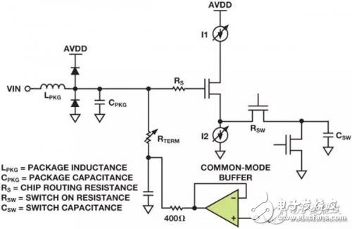
Figure 2. Equivalent circuit for buffering RF sampling ADC input
Regardless of the architecture used, the absolute maximum voltage that can be sustained at the ADC input is determined by the voltage that the MOSFET can handle. Buffered inputs are more complex and consume more power than unbuffered inputs. ADC has many different types of buffers, the most common one is the source follower.
Failure mechanismThe failure mechanisms of buffered and unbuffered ADCs are different, but they usually fail when the maximum allowable gate-source voltage ((VGS)) or drain-source voltage ((VDS)) is exceeded. These voltages are shown in Figure 3.

Figure 3. Key voltages of MOS transistors
For example, assuming that VDS exceeds the maximum allowable voltage, a VDS breakdown fault occurs, which usually occurs when the MOSFET is off and an excessive voltage is applied to the drain relative to the source. If VGS exceeds the maximum allowable voltage, it will cause VGS breakdown (also known as oxide breakdown). This usually occurs when the MOSFET is in the on state and an excessive voltage is applied to the gate relative to the source.
Failure mechanism of unbuffered ADCFigure 4 shows an unbuffered ADC input. The sampling process is controlled by inverted clock signals Φ and Φ, which are the sample / hold signal of MOSFET M1 and the reset signal of MOSFET M2. When M1 is on, M2 is off, and the capacitor CSW tracks the signal (sampling or tracking mode). When M1 is turned off, M2 is turned on after the comparator in the MDAC makes a judgment, and the capacitor CSW is reset. This makes the sampling capacitor ready for the next sampling during the sampling phase. The circuit usually works well.
However, the high voltage input exposes M2 to stresses that exceed its drain-source voltage. When the input high voltage is sampled (M1 is turned on, M2 is turned off), M2 will be exposed to a large VDS, which is in the off state in less than half the sampling clock period, but even if it is only a momentary exposure Will reduce the reliability of the circuit, resulting in ADC failure over time. In reset mode (M1 is off, M2 is on), because of the input signal on the drain of M1, it will also be exposed to a large VDS voltage.

Figure 4. Failure mode of unbuffered ADC input
Buffer ADC failure mechanismFigure 5 shows a buffered ADC input. The same clocking scheme applies to sampling and reset signals. Regardless of the phase, when the gate of the buffer M3 is exposed to the high voltage input, currents I1 and I2 are generated. The current source I1 is implemented using PMOS transistors, while I2 is implemented using NMOS transistors. The high voltage on the gate of M3 causes the I1 and I2 MOSFETs to generate excessive VDS. In addition, the high voltage on the gate of M3 can also cause breakdown of the oxide layer.

Figure 5. Failure mode for buffered ADC input
The breakdown mechanisms of buffered and unbuffered ADCs are different, so the absolute maximum input voltage is also different, as shown in Table 1.
Air conditioning appliances, automatic control system is commonly used in the device, generally used to switch on and off the circuit, is an important component of automatic control and remote control circuit.
Air Conditioning Relay,Air Conditioning Time Delay Relay,Household Fan Air Conditioning Relay,Energy Efficiency Air Conditioning Relay
Ningbo Xingchuangzhi Electric Appliance Co.,Ltd. , https://www.xingchuangzhi.com