
The source of aliasing: This point is explained in the Nyquist theorem. Nyquist's theorem states that when a time-continuous signal is converted into a discrete signal, it needs to be sampled more than 2 times in a cycle. If the sampling times are not enough, the lost information cannot be recovered. You can see this more clearly from Figure 1. If the signal is sampled once per cycle, all you get is a DC signal (the amplitude is arbitrary), as shown in Figure 1a. If you sample twice per cycle, you get a square wave signal (Figure 1b). It is worth noting that sampling the input signal twice per cycle is a very special case, which should be avoided at all times. Figure 1c shows a case where a 190kHz signal is sampled at a 200kHz sampling rate. The resulting signal is a good sine wave, but the frequency is wrong. The frequency change is caused by the aliasing phenomenon.
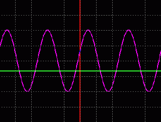
Figure 1a. When the sinusoidal signal is sampled once per cycle, a DC signal with an arbitrary amplitude is obtained.
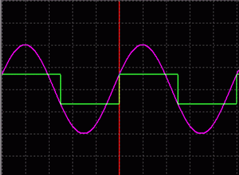
Figure 1b. The same sine wave is sampled twice per cycle to obtain a square wave, and the amplitude information is lost.
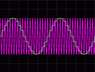
Figure 1c. Fsignal = 190kHz and Fs = 200kHz are under-sampled signals, and the result is caused by aliasing.
Figure 2 shows the representation in the frequency domain. As can be seen from the figure, signals with frequencies higher than f> fs / 2 are mirrored to fs / 2. To avoid this phenomenon, it must be ensured that there are no higher frequency components in the signal. Therefore, we must understand the highest frequency of the signal, the sampling frequency needs to be higher than twice this frequency. One of the most original considerations is to solve this problem from the digital domain, but this is obviously not desirable, because once the signal is sampled and some signals are aliased into the frequency band of interest, these frequency components cannot be removed from the signal. Anti-aliasing filtering must be performed in the analog domain, that is, before the signal is sampled.
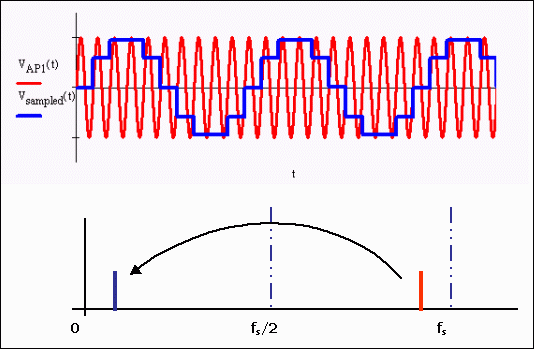
Figure 2. Aliasing in the frequency domain, undersampled signals are mirrored to fs / 2.
Next step-design anti-aliasing filter. Designing an anti-aliasing filter requires first determining the desired filtering characteristics (cutoff frequency, transition band attenuation, etc.), and then selecting the best filtering scheme (sometimes called the filter type) that meets the application requirements. In general, oversampling is used, and the higher the oversampling frequency, the easier the filter design. However, oversampling requires a higher rate ADC, and the cost is higher.
For example, when the oversampling factor is 8, the sampling frequency is eight times the highest signal frequency. This achieves a better compromise between ADC cost and filter complexity. Assuming that the ADC resolution is 14 bits, it can provide a signal-to-noise ratio (SNR) of 80dB. At half the sampling rate (here, 4 times the signal frequency), the low-pass filter needs to provide 80dB of attenuation to ensure that all spurious signals are adequately attenuated and will not appear in the sampled signal. This means that 40dB of attenuation per octave needs to be provided in the transition band, and higher order filters are required to meet this design requirement. The 7th order Butterworth filter can meet the above requirements, but it is not the best choice for specific applications. Different filter types can be selected for different applications. Figure 3 shows the frequency response characteristics of Butterworth filter, Chebyshev filter and elliptic filter. It can be seen from the figure that they have different characteristics of pass band and transition band. Compared with Butterworth filter, the elliptic filter has a steeper transition band, but its phase frequency characteristic is worse. The type of filter should be selected according to the specific application. For ordinary data acquisition systems, Butterworth filter (or Bessel filter) can be used. If the phase accuracy is not high, Chebyshev or even ellipse can be selected. filter.
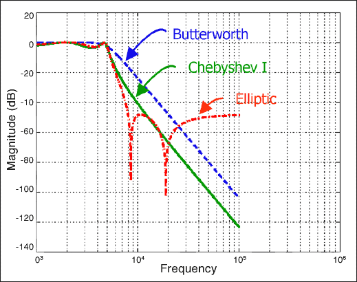
Figure 3. Comparison of frequency response of different filters
General-purpose A / D converters are: SAR (successive approximation) ADCs for medium rates; flash ADCs for high-speed to ultra-high rates; and Σ-Δ ADCs for low-speed systems. They all require anti-aliasing filters. The filter requirements depend on the conversion rate and the desired input bandwidth, but the sigma-delta ADC is special. This conversion technique uses a very high input sampling rate and conversion rate, and subsequent digital filtering reduces the effective throughput rate, which affects the resolution (dynamic range) improvement. The requirements of the Σ-Δ ADC for anti-aliasing filters are related to the ratio of the input sampling rate to the highest signal frequency. This reduction in demand is also manifested in other oversampled data converters. In this case, a simple RC filter. Selecting a simpler anti-aliasing filter will result in a longer transmission delay, which increases the design difficulty for converters that use closed-loop control or multiplexing.
Because analog filters have certain design difficulties and large tolerances, and are difficult to manufacture, especially for products with compact spaces, many designers are reluctant to use analog filters. A good criterion for measuring the error is to assume that the tolerance of the separation element is doubled, so that if standard commercial resistors and capacitors are used, it will cause a large error in the corner frequency and transition band. The best way to solve this problem is to choose an integrated filter solution, which can be obtained from companies such as Maxim.
There are two types of integrated filters: continuous-time filters and switched capacitor filters. Continuous-time filters usually require external components to adjust the angular frequency, which limits their flexibility. The switched capacitor filter can be used flexibly according to its structure. In general, it can replace a separate or integrated continuous-time filter.
The switched capacitor filter is a filter structure that has been recognized for a long time and can be reliably integrated using current silicon process technology. Its working principle and mathematical derivation are shown in Figure 4. The working principle is: under the control of the switch at both ends of the capacitor, the capacitor is charged and discharged. This charge transfer process generates a pulse current, and the average current can be calculated. When the switching frequency is fast enough, the current is equivalent to the current flowing through the resistance, which can be regarded as the resistance is replaced by a capacitor. The current and indirect resistance values ​​depend on two factors: the size of the capacitor and the switching frequency. The higher the switching frequency and the larger the capacitance value, the larger the current, or the smaller the resistance value. If this filter structure is used, the frequency characteristics will change with the change in the size of the capacitor or the switching frequency. In the integrated scheme, the capacitance value is fixed, and the filtering characteristics are controlled by the switching frequency. The principle of this filter is shown in Figure 5.
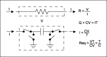
Figure 4. Functional block diagram of switched capacitors
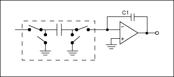
Figure 5. A simple filter using switched capacitor technology
The accuracy of the filter depends on the tolerance of each component. In the separation scheme, we can only use components with inconsistent tolerances. In the integrated solution, high component consistency can be guaranteed (within 0.1%). Therefore, we can control the frequency response characteristics of the integrated filter well. For example, the MAX7490's angular frequency accuracy can reach 0.2%, while using separate components can not achieve this index. In addition, the integrated solution also has excellent temperature characteristics, the temperature drift coefficient can reach 10ppm / ° C.
It is also necessary to point out the sampling of the signal by the switched capacitor scheme, which converts the time continuous signal into a time discrete signal, which means that we have to consider the aliasing problem again. Thankfully, the sampling rate of this filter is very high, usually 100 times oversampling. Therefore, only a simple RC filter is needed. Another problem to consider in the system is: the distortion caused by the phase jitter of the switching clock, which is the same as the problem in the ADC. Figure 6 shows a situation where the correct signal is erroneously sampled, leading to a certain amplitude error.
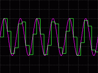
Figure 6. Amplitude distortion caused by undersampling
There are two forms of clock jitter. If the phase error is random, the noise floor will increase; if the jitter is periodic, the distortion (THD) will increase. Jitter is an amount of time, for example: ps peak-to-peak or RMS. In order to achieve a certain signal purity, can we tolerate many large jitters? Reference 1 points out that for a 16-bit system, 1nspp (peak-to-peak) clock jitter will reduce the SNR from 98dB to 91dB. In order to limit the impact of jitter to 0.5dB, the jitter cannot be higher than 400pspp.
Using a commercial clock oscillator can easily meet the requirements of the above jitter indicators, such as: SaRonix NTH5, jitter is only 8psRMS (53pspp). The disadvantage of this solution is that it limits the signal frequency. In most systems, other devices (such as ADC, µC, etc.) also need to provide a clock. If these clocks are generated with other oscillators, these clocks will be out of synchronization and will cause many other problems. MAX7375 or DS1085 can generate multiple clocks, and they are synchronized with each other, and can provide better jitter indicators (160ps and 300ps, respectively), can achieve signal purity of more than 90dB. Another advantage of using this device to provide a clock is: programmable different clock frequencies. That is, an analog filter with software programmable frequency response characteristics can be obtained, thereby creating an extremely flexible system.
Figure 7 is a data acquisition system solution based on the above discussion. The ADC has a 14-bit resolution and a sampling rate of 200ksps (MAX1067 series). The device requires at least 24 clocks per conversion. The anti-aliasing filter uses the MAX7418-21 series products, which provide various filter types, such as Bessel, Butterworth, and ellipse. The corner frequency is set to 1/100 fClk. Considering that the DSP controls the sampling of the converter (only one timer is required), the same clock can be used for the filter and ADC, fully synchronized. Using DS1085 to generate the clock can get two clocks, and the second clock can be used for DSP. DS1085 is programmed through a 2-wire interface. When the system works at different sampling rates, the frequency can be reset and the same PCB can be used to achieve different functions.
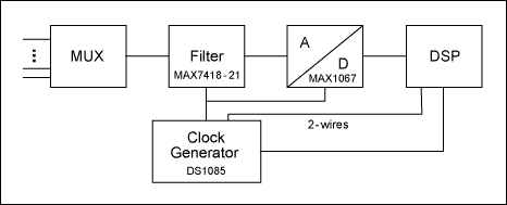
Figure 7. Functional block diagram of the data sampling system
In the circuit shown in Figure 7, the cooperation between the devices is acceptable in terms of cost and complexity. Another advantage is programmability, which provides great flexibility, which simplifies the design and reduces costs.
When people talk about 7inch tablet, kids appears on their minds, especially for elementary students or kindergarten kids for playing intelligent exploitation games or online learning. Clients usually choose 7 inch tablet wifi only as 7 inch educational tablet for project, wifi one is much cheaper. Of course, 7 inch Android Tablet with 3G lite or 4G lite also optional. You can always see a right tablet at this store, no matter amazon 7 inch tablet, 8 inch android tablet, or 10.1 android tablet.
Except android tablet and window tablet, there are Education Laptop, Mini PC , All In One PC, which are is the main series at this store. Any other special configuration interest, just email or call us, you will receiving value information in 1-2 working days.
To meet clients` changing requirements, we contributes 10-20% profit to develop new designs according market research and client`s feedback.
So you are always welcome if can share your special demand or your clients opinion for the products.
7 Inch Tablet,7 Inch Android Tablet,Amazon 7 Inch Tablet,7 Inch Tablet Wifi Only,7 Inch Educational Tablet
Henan Shuyi Electronics Co., Ltd. , https://www.shuyipcs.com