
PCB as a carrier of various components and circuit signal transmission hub has become the most important and critical part of electronic information products. The quality and reliability of the PCB determine the quality and reliability of the whole equipment.
With the miniaturization of electronic information products and the environmental protection requirements of lead-free and halogen-free, PCBs have also developed toward high density, high Tg, and environmental protection. However, due to cost and technical reasons, PCBs have experienced a large number of failures during their production and application, and this has led to many quality disputes. In order to clarify the cause of the failure in order to find a solution to the problem and to clarify the responsibility, a failure analysis must be performed on the failed case.
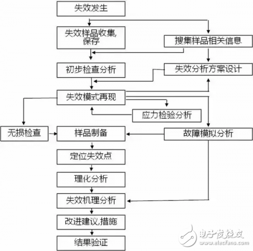
Failure Analysis Basic ProcedureTo obtain the exact cause or mechanism of a PCB failure or defect, the basic principles and analysis flow must be followed, otherwise valuable invalidation information may be missed, causing the analysis to continue or possibly obtaining erroneous conclusions. The general basic process is that, based on the failure phenomenon, information collection, functional testing, electrical performance testing, and simple visual inspection must be performed to determine the failure location and failure mode, that is, failure location or failure location.
For a simple PCB or PCBA, the failure location can be easily determined. However, for a more complex BGA or MCM packaged device or substrate, the defect is not easily observed by the microscope. It is difficult to determine for a moment, and this time needs to be determined by other means.
Then we need to analyze the failure mechanism, that is, use various physical and chemical means to analyze the mechanism that leads to PCB failure or defects, such as welding, contamination, mechanical damage, moisture stress, medium corrosion, fatigue damage, CAF or ion migration, Stress overload and so on.
Then, the failure analysis is based on failure mechanism and process analysis to find the cause of the failure mechanism. If necessary, test verification is carried out. Generally, the test should be performed as far as possible, and the exact cause of induced failure can be found through the test verification.
This provides a basis for targeted improvement of the next step. Finally, according to the experimental data obtained from the analysis process, facts and conclusions, the failure analysis report was prepared. The report requires clear facts, strict logical reasoning, and strong rationality.
During the analysis process, pay attention to the basic principles that the analysis method should be used from simple to complex, from outside to inside, never to destroy samples, and then use destruction. Only in this way can we avoid losing key information and avoid introducing new artificial failure mechanisms.
Just like a traffic accident, if a party to the accident destroys or flees the scene, it is difficult for a clever policeman to make an accurate determination of liability. At this time, the traffic regulations generally require that the person fleeing the scene or destroying the scene bear full responsibility.
The same is true for the failure analysis of PCB or PCBA. If soldering iron is used to repair the failed solder joints or if large shears are used to sharply cut the PCB, reanalysis will be impossible. The failure site has been destroyed. Especially in the case of a small number of failure samples, the true failure cause cannot be obtained once the failure site environment is destroyed or damaged.
Optical microscope
The optical microscope is mainly used for the appearance inspection of the PCB, looking for the location of failure and related physical evidence, and initially determining the failure mode of the PCB. The appearance inspection mainly checks the PCB for contamination, corrosion, the location of the explosion board, the circuit layout, and the regularity of failure. If it is batch or individual, is it always concentrated in a certain area?
X-ray (X-ray)
For some parts that cannot be visually inspected and the through holes inside the PCB and other internal defects, the X-ray fluoroscopic system has to be used for inspection.
The X-ray system uses different principles of different material thickness or different material density to absorb X-rays or transmit light. This technique is more used to inspect defects inside PCBA solder joints, internal defects in through-holes, and positioning of defective solder joints in high-density packaged BGA or CSP devices.
Slice analysis
Slicing analysis is the process of obtaining the PCB cross-section structure through a series of means and steps such as sampling, inlaying, slicing, polishing, etching, and observation. The slicing analysis can provide a wealth of information reflecting the microstructure of the PCB (through-hole, plating, etc.), providing a good basis for the next step in quality improvement. However, this method is destructive. Once sliced, the sample must be destroyed.
1.Power Bank For Hero 11/10/9/8/7/6/5 Battery Charge battery .Charge phone .Charge devices.
2.Unique Design For Hero batteries Innovative power bank for "Storage + Charging' Auto power off when full charged, eficient and safe With a free battery tray Compatible with Hero 8/7/6/5 batteries
3.10000mAh Samsung high-capacity density battery cells Adopt high quality 10000mh battery cell comply with national portableLi-ion battery Safety standard GB31241-201 it can charge iphone 14 up to twice.
4.Three ports output at the same time.Up to 3 simultaneous charging at the Hero battery USB-C and USB-A ports.
5.There is even a low current mode with automatic recognition when plugged in, suitable for mobile phones / bluetooth headsets / outdoor lights outdoor speakers etc.Plug and play.
6.PD 20W Fast charging Less waiting.
7.More Safe protections for Charging Protection for every use,solving the concern of safety hazards.
8.Help you when shooting outdoors.Airline compliant, it can be taken with you on planes and trains, outdoor camping.hiking, travelling and
shooting without anxiety.
Power bank, mobile power bank, portable power charger
Mietubl Global Supply Chain (Guangzhou) Co., Ltd. , https://www.mietublmachine.com