
STM8S IO multiplexes are more complicated to configure with the program code, generally operate flash to operate opTIon byte bytes, configure the register more cumbersome, you can use the STM standard peripheral driver library to set. This article uses an interface configuration to configure IO multiplexing pins, which uses STVP to configure. Because the data saved in FLASH is not lost during power-down, the OPTIon Bytes can be erased by STVP, and then the STVD emulator can be used to program the IO multiplex.
Program mode IO multiplexing see here

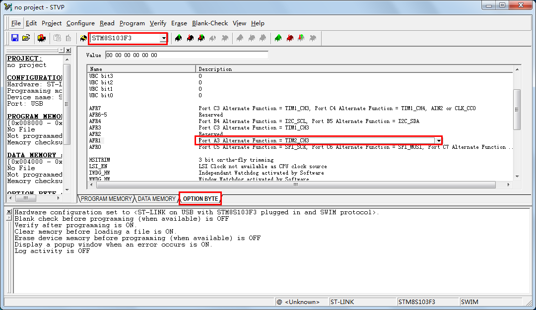
[step1] Open STVP software
[step2] Open the xxx.s19 file we need to download, CTRL+F5 (File->Ram Exec)
[step3] Configure Needed Multiplexed Pins
The main configuration of the multiplexing function of the IO port is AFR0-AFR7. Here we configure the multiplexing of the PWM output pin of the timer TIM2_CH3 channel. By default, PD2 is the output, and it is configured to be multiplexed as the PA3 output. As shown above, select PA3 in the pull-down menu in AFR1.
[step4] Download the program to STM8S, Progam-"All tabs. This realizes the IO multiplexing configuration.
3 test procedures/*
TIM2_CH3 PWM
PD2 output
*/
#include "STM8S103F3P.h"
Void CLK_init(void)
{
CLK_ICKR |= 0X01; //Enable internal high-speed clock HSI
CLK_CKDIVR |= 0x08; // 16M Internal RC is divided by 2 and the system clock is 8M
While(!(CLK_ICKR&0x02));//HSI is ready
CLK_SWR=0xe1; //HSI is the main clock source
}
Void Init_Tim2(void)
{
TIM2_CCMR3 |= 0X70; // Set timer 2 three-channel (PD2) output compare three modes
TIM2_CCMR3 |= 0X04; //Output Compare 3 Preload Enable
TIM2_CCER2 |= 0x03; // Channel 3 enabled, active low, configured as output
// Initialize the clock divider to 1, that is, the clock frequency of the counter is Fmaster=8M/64=0.125MHZ
TIM2_PSCR = 0X06;
// Initialize the autoload register to determine the frequency of the PWM square wave, Fpwm=0.125M/62500=2HZ
TIM2_ARRH = 62500/256;
TIM2_ARRL = 62500%256;
// Initialize the compare register to determine the duty cycle of the PWM square wave: 5000/10000 = 50%
TIM2_CCR3H = 31250/256;
TIM2_CCR3L = 31250%256;
// start counting; update disabling
TIM2_CR1 |= 0x81;
//TIM2_IER |= 0x00;
}
Void Init_GPIO(void)
{
/* is set to push-pull output, PD2 is connected to the LED light */
PD_DDR |= 0X04; //Set PD2 port to output mode
PD_CR1 |= 0X04; //Set PD2 port to push-pull output mode
PD_CR2 &= 0XFD;
PA_DDR |= 0X08; // Set the PA3 port to output mode
PA_CR1 |= 0X08; //Set PA3 port to push-pull output mode
PA_CR2 |= 0XF7;
}
Void main(void)
{
CLK_init();
Init_GPIO();
Init_Tim2();
While (1);
}
Dry-Type Transformers,Dry Transformer,Dry Type Power Transformer,Dry Distribution Transformer
TRANCHART Electrical and Machinery Co.,LTD , https://www.tranchart-electrical.com