
Translation: Changjiang Electronics Technology Co., Ltd. Dr. Chen Lingzhi. Dr. Chen has been engaged in MIS substrate technology research for many years and is one of the promoters of MIS substrate packaging technology.
MIS has emerged as a new type of packaging in areas such as analog, power ICs, and digital currency. IC packaging based on an emerging technology MIS is accumulating momentum. ASE, Carsem, JCET, STATS ChipTAC, Unisem, and others are all developing IC packaging technology based on MIS substrates. Currently, they are used in analog and power ICs. And market sectors such as digital currency have developed rapidly.
The MIS package uses a proprietary substrate material that has been primarily used in some specific IC packages. MIS substrates are currently being developed and sold by a number of suppliers, so packaging companies can purchase from multiple vendors and then IC packages. Some people think that MIS substrate is a kind of lead frame. Unlike conventional substrates, MIS includes one or more prepackaged structures. Each layer is interconnected by electroplating copper to provide an electrical connection during the packaging process. MIS supports single-chip or multi-chip packages, providing solutions for ultra-thin, high-density fine-pitch packages. It can be used to develop advanced lead frame packages, flip-chip packages, module packages, and system-level packages.

Figure 1: Pre-packaged MIS lead frame
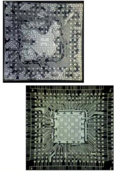
Figure 2: MIS-based IC package
On the surface, MIS is similar to a fan-out wafer-level package. The biggest difference between them is that MIS is slightly inferior in terms of I/O and density. Therefore, in the actual use of packaging, MIS mainly competes with some mature midrange packages.
MIS has existed for nearly a decade, but the market has just begun. "(MIS) is suitable for both high and low power applications due to its advanced wiring capabilities and reliability," said Mark Gerber, director of technology marketing at Sun Moonlight.
In addition, MIS provides customers with a new package option and a potential alternative to existing packages. "Production volume has been rising in recent years," said Nokibul Islam. "You can use MIS instead of some traditional QFN or leadframe-based packages because MIS has finer routing capabilities, better electrical and thermal performance, and a smaller form factor." Also, MIS packages are locked. The package used for digital currency chips enters the digital currency server market. The volume of this market is very large. Of course, there are also some people who are beginning to consider whether or when the digital money market may end. What is MIS? MIS was developed around 2010, and Changjiang Electronics was one of the earliest developers, and then licensed this technology to its sister company, MISpak. MISpak develops and sells MIS materials to packaging plants (OSAT). Other MIS substrate suppliers include ASM, PPT, QDOS, and SIMMTECH. Therefore, there are more options for packaging plants to purchase MIS substrates. Then, during the packaging process, the chip is placed on the MIS substrate for packaging, and finally the MIS package is formed.
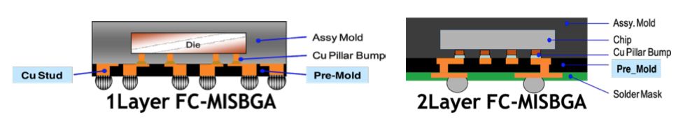
Figure 3: Flip Chip MIS BGA Package (FC-MISBGA)
With the passage of time, the scale of MIS business began to grow rapidly. In 2017, only the MISpak family expects to ship 2.5 billion units. In 2010, only 20 million units were shipped. In the area of ​​MIS packaging, MISpak claims that it has about 30 end customers. Of course, this does not include the shipments of other MIS suppliers.
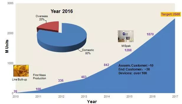
Figure 4: Shipment of CMOS ICs
MIS differs from conventional IC package substrates. The traditional package uses an organic substrate, which is a multi-layer substrate technology based on PCB materials. In the package, the chip is placed on the substrate. "The characteristic of MIS technology is that it is developed from the encapsulation technology. In the MIS substrate, the copper wiring is embedded. Therefore, the embedded structure can be more detailed wiring," said Nokibul Islam. . MIS also has some other features. "It uses encapsulants as insulation between layers," said Mark Gerber. "When you use this type of leadframe and encapsulate it here, the encapsulated material of the package is similar to the material properties of the leadframe. Therefore, it is very good from the point of view of moisture absorption or function." There are many ways to make MIS substrates. MIS first appeared in the shape of a long strip of size 250mmX70mm. MIS fabrication requires a series of process steps such as etching, polishing, lithography, encapsulation and electroplating. For example, a single-layer MIS process often begins with a carrier board. "On the metal carrier plate, the wiring of the substrate is made by electroplating copper," explains Nokibul Islam. "So after the copper plating is completed, the next step is to remove the photoresist film process." After removing the film. "The envelope was started. The encapsulant was then ground to thin it to the required thickness. The carrier was finally etched," said Nokibul Islam.
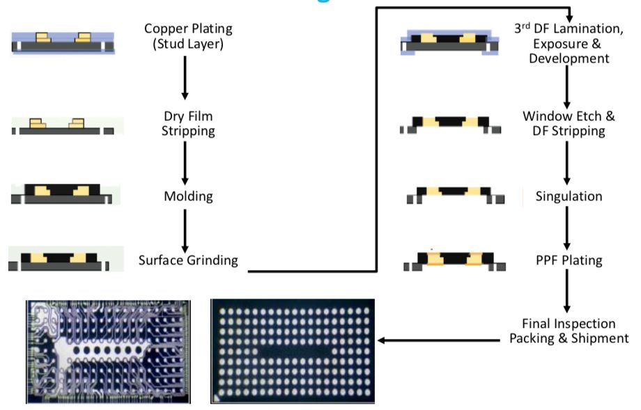
Figure 5: MIS substrate manufacturing process flow
For MIS packages, the most advantageous technology for this MIS package is thin, I/O packages between 150 and 200. However, this technology is limited by a line width of about 25 μm, which means that it is mainly intended for mid-range applications. The line width spacing refers to the metal wiring in the package.
In comparison, the fan-out package (Fan-Out), which is mainly used for high-end applications, has the following standard densities: I/O is less than 500, and its line-to-line spacing is more than 8μm. In a high-density fan-out package, Its I / O is greater than 500, line width is less than 8μm. At the same time, the MIS material itself is relatively thin. Such substrates are prone to warp and uniformity problems during the packaging process. The issue of output and cost is another issue. “Different application requirements require special packaging materials for design flexibility and package thickness,†said Ho Kwok Kuen, vice president of marketing at ASM Materials. "Compared with lead frames, ABiT-MIS has the ability to produce high-precision and complex-lined pre-packaged substrates. However, in order to achieve the resolution of the design, more process steps are required, so in order to achieve the target of the yield of the final product, We need to pay great attention to how to achieve higher yields in each process.
In addition to the equipment, ASM also provides lead frame and MIS packaging materials. This refers to ASM, ASM Buildup Interconnect Technology. Despite all the challenges, the MIS market has grown rapidly. "In the past two years Here, we have seen many customers want to use MIS packages to meet the needs of digital currency mining applications. "Ho said," MIS not only has an ever-increasing market share in radio-frequency encapsulation in the communications sector, but also has a growing demand for power management and automotive applications. At the same time in the market, MIS is also facing fierce competition. This refers to "Fan-Out" technology, although MIS will not compete with Fan-Out technology. In fact, MIS is mainly competing with lead frame package and LGA package. " The application area of ​​MIS is mainly between the standard QFN package and a simple double-layer substrate. "Gil Chiu, vice president of Yuxin North America, said. The leadframe package includes several package types, such as quad flat no-lead (QFN) and quad flat pack (QFP). The lead frame is a metal frame, the chip is attached to the frame, and the thin wire is used. Make a connection.
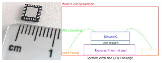
Figure 6: QFN package
Source: Wikipedia
QFN is a mature, low-cost and reliable packaging method. Therefore, QFN has huge demand in the analog, automotive, Internet of things, and RF markets. Generally speaking, although QFN is a single-layer technology with limited I/O capacity, "If you can implement it with QFN, you obviously do it because QFN costs less than MIS," Chiu said. "But when you use QFN, you have to accept spacing restrictions." MIS also competes with LGA packaging technology. The LGA has an array of metal pads for connection at the bottom of the package. LGA is suitable for modules, processors and other products.
Figure 7: Power Module LGA Package Structure
MIS is cheaper than LGA but has fewer features. However, Yuxin believes that LGA is sometimes affected by high material costs, connection molding (Via) molding costs, and so on. Therefore, QFN and LGA have some disadvantages. Here is where MIS comes into play. For example, an IC design company may have a ready-made chip design at a given process node, and the chip package uses a QFN package. In this hypothetical example, suppliers face some challenges. "Customers basically say I have a ready-made solution. I don't want to change my chip. I don't want to shrink my chip, but I want to shrink my package. I want a thinner, smaller package." Said Chiu.
An effective solution is to move from QFN packages to MIS packages. Usually, you can use the same chip as the lead frame package and use it for MIS package. The MIS package can be similar to the QFN package, but the MIS can have more I / O and better performance. The MIS package can be basically the same as other package types, such as flip chips, modules, and SiPs. "The MIS technology is different. It is essentially a lamination process. It allows you to achieve denser metal routing. Therefore, you can shrink the package while maintaining the same chip size," said Chiu. "Using MIS, customers do not have to spend time or resources to redesign a smaller chip and do not have to shrink the chip's appearance. With MIS, you can make the product get extra. It allows you to keep up with the ready-made solution. So, MIS You can provide a smaller package at the same cost." "Catch" or "miss"? For some time, some OSAT plants have been shipping MIS packages. However, each supplier has a different strategy.
Changjiang Electronics/Xingke Jinpeng has shipped all kinds of chip-on-lead, FC, module and SiP package products based on MIS technology. "MIS has its specific advantages. The best is a high-power, high-thermal application with low I/O count," said Chang Electric's Islam. So far, the industry's main shipment is single-layer MIS packages with 25/25μm linewidth. "For the future market, we are currently working on a higher resolution, which means a finer line width and a thinner profile," said Islam. “Two years later, it can achieve 15/15μm linewidth.†In addition, Changjiang Electronics/Singapore and other manufacturers are fully committed to the Ajinomoto-based ABF (Ajinomoto Build-up Film) membrane technology. The more advanced craftsmanship. Using laser molding and direct electroplating of copper, ABF enables MIS to achieve multi-layer substrates with a line-to-line spacing of 12/12 μm, enabling multilayer, triple, and four-layer multilayer packaging.
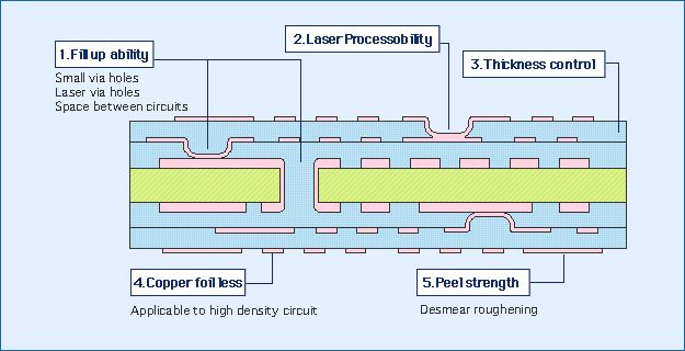
Figure 8: Ajinomoto's ABF membrane
"Using ABF membranes, the MIS process is basically the same. We just use thicker ABF membranes instead of encapsulants. We can provide this type of multi-layer MIS substrate," he said. "At the end of this year, we will start using two- or three-layer MIS substrates based on ABF film." Sun Moonlight's MIS package is also growing. Sun Moonlight’s MIS technology is called C2IM/MIS. "MIS allows you to make packages that have the same fine-pitch routing capabilities as QFN packages," said Moonlight's Gerber. "(Some customers) are very insistent on using QFN packages, but there is a limit to the routing capability. When you can do 20/20μm or 30/30μm routing, this will provide them with a layer of wiring metal solutions." In addition to C2IM/MIS, Riyueguang offers another competitive technology called "ChipLast fanout package," which is different from current fanout packages. "It's essentially a post-chip process, which means it's a flip chip process," Gerber said. "The ChipLast fan-out package is a coreless substrate process that uses two different insulating materials depending on the wiring density and only one metal wiring."
In addition, relative to the MIS substrate, Sun Moonlight has another option called aS3+. "The aS3 + is an embedded circuit (ET) coreless organic substrate, this technology can also provide a similar advantage with the C2IM / MIS scheme. In addition, aS3 + / ET substrate can do three or more layers of wiring, and C2IM/MIS is relatively lacking in this regard," he said. "The aS3 + / ET can use conventional insulating material or ABF insulating material. At the same time, because it does not require core material and its manufacturing process flow and its inherent structural features, it can provide ultra-low inductance between layers that facilitates higher speed connections. At the same time without losing cost competitiveness and reliability." For Yuxin, they see three applications of MIS packaging. These packages can achieve a total thickness of 0.33 mm or less. The first application is what the company calls a cavity. The chip is packaged in the cavity of the package.
“We are using MIS to implement a fine-pitch chip flip-chip package between the substrate package and the QFN package, which can be demonstrated in this regard,†Yu Yu’s Chiu said. "We are also considering the use of MIS for system-level packaging, which is a lower-cost solution for LGA standard module packaging." For MIS, the biggest market is power/power ICs. Another driver is the digital currency IC package. Looking ahead, MIS may exceed these markets. "The good news is that we are seeing more and more conventional products are also considering whether to use MIS package." Chiu added.
Neodymium Tweeter,Tweeter Horn Driver,Neodymium Compression Driver,Neodymium Speaker Drivers
Guangzhou Yuehang Audio Technology Co., Ltd , https://www.yhspeakers.com