

Equivalent Circuit:
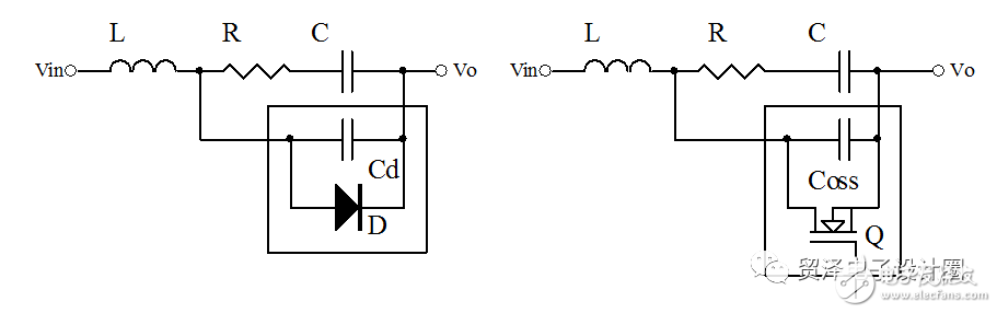
L: sum of stray inductance such as transformer leakage inductance and component lead inductance.
R, C: Absorb resistor and capacitor.
D, Cd: Rectifier diode, Cd is the junction capacitance of D.
Q, Coss: Switching MOSFET, Coss is the junction capacitance of the MOSFET.
When the switch tube is turned on to off due to the leakage inductance L, its energy is absorbed by R and C. Otherwise, a spike voltage will affect the reliability of the component and cause EMI.
There is also a problem of reverse recovery current when the rectifier diode is turned off, but when the reverse recovery current is maximized, it is regarded as the starting point of the analysis. In the actual analysis, the process is still the same, but the initial state is different.
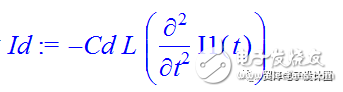
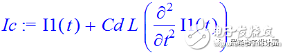
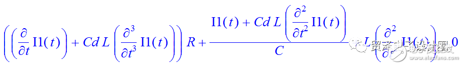
Consider the circuit of the rectifier diode, and set the current flowing through L to I1(t):
The current flowing through the junction capacitor Cd is
The current flowing through the snubber capacitor C is
The calculus equation is obtained according to the voltage across the Cd equal to the voltage across R and C:
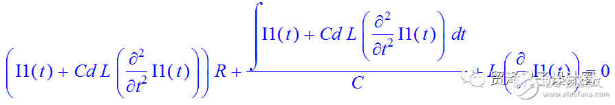
Because of the integral, the equation is inconvenient to solve, and it is derived to obtain a third-order differential equation:
Since Cd is small, it can be ignored to simplify the analysis, resulting in a simplified differential equation:

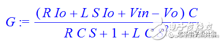
Consider the initial state I1(0)=Io, I1'(0)=(Vin-Vo)/L, where Io is the maximum value of the current when the switch is closed, and the transformed equation is obtained by applying the Laplace transform:
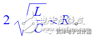
This is a 2nd-order system and should be operated in an over-damped state to prevent oscillations. Therefore, it is necessary to ensure that the pole has two distinct real roots.
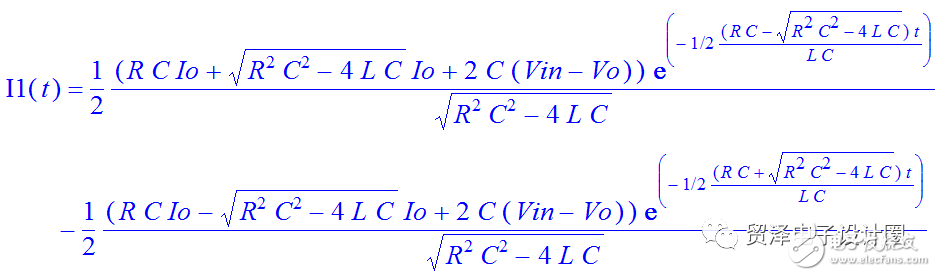
The solution of the current I1(t) can be obtained by applying the inverse Laplace transform:
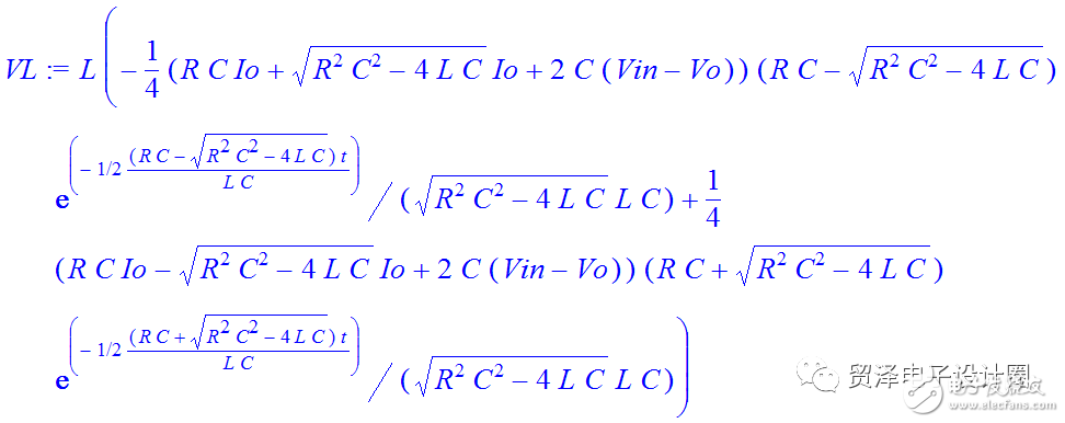
Voltage on inductor L:
Voltage on diode D:

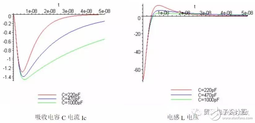
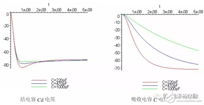
Assume L=0.1uH, C=220pF, Vo=12V, Vin= -60V (when MOSFET is ON, transformer secondary voltage is reversed, Vin is changed from 12V to -60V), R=2*sqrt(L/C ) = 42.6 ohms.
Io=0 in the DCM state, considering the effect of different R values ​​on the waveform:
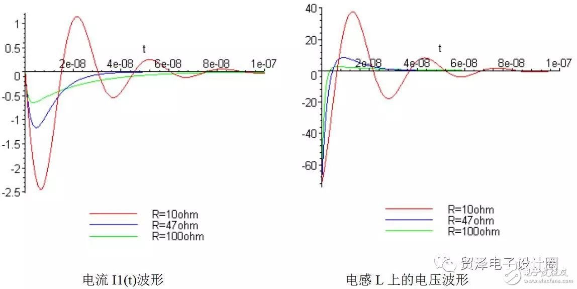
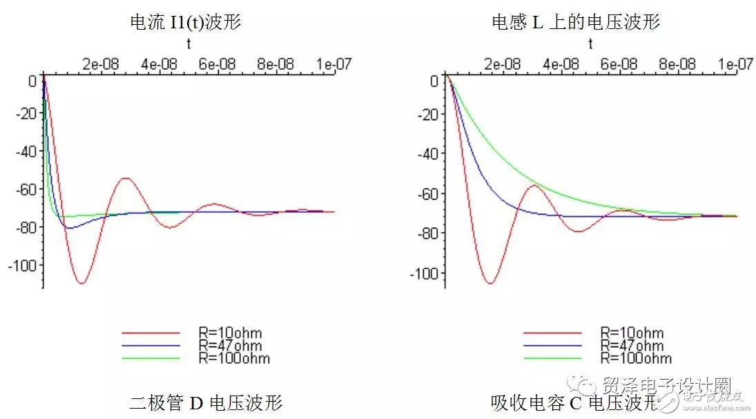
It can be seen that the smaller the resistance is, the more the waveform of the voltage and current oscillates, and the higher the peak value, the easier it is to adversely affect the loop. Therefore, to ensure that the operation is in an over-damped state, the resistance R cannot be made small.
Consider the effect of different capacitance C on the waveform when R=47 ohm:

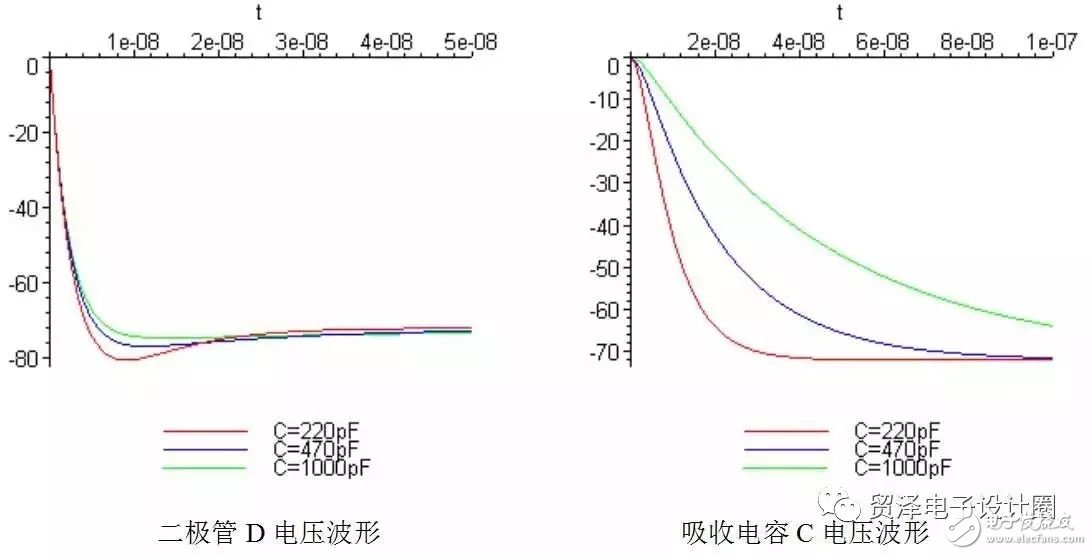
It can be seen that the larger the capacitance C, the lower the voltage current rate and the voltage overshoot will be, which will benefit EMI, but the peak current will become larger.
Consider the power consumption at resistor R at this time, assuming a loop operating frequency of 50 KHz:
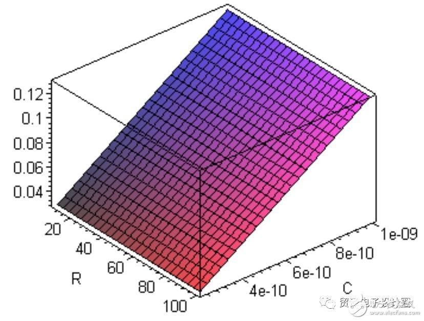
It can be seen that the power consumed by the absorption resistor under normal conditions is independent of the value of R, and is only related to the voltage across C and C. Therefore, it can be seen that improving EMI is at the expense of increasing power consumption, which reduces the overall efficiency of the loop. C can't take too much, at this time P=1/2*C*(Vin-Vo)^2*f.
It is necessary to see that the absorption circuit absorbs not the energy on the leakage inductance L, but the energy generated by the voltage jump on the capacitor C.
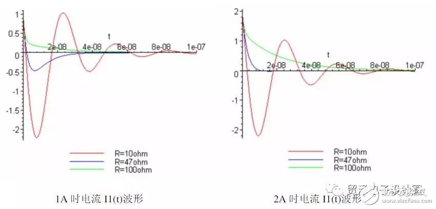
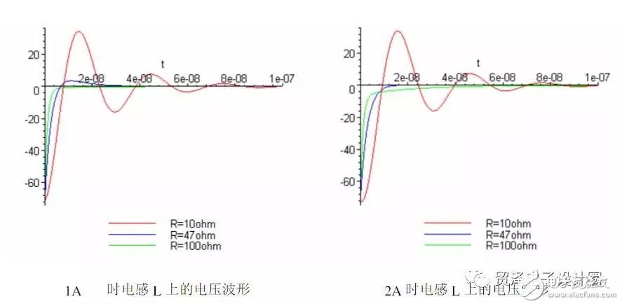
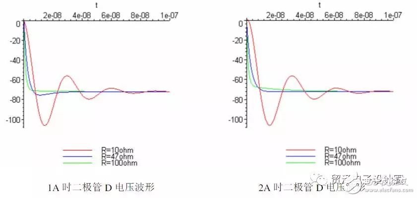
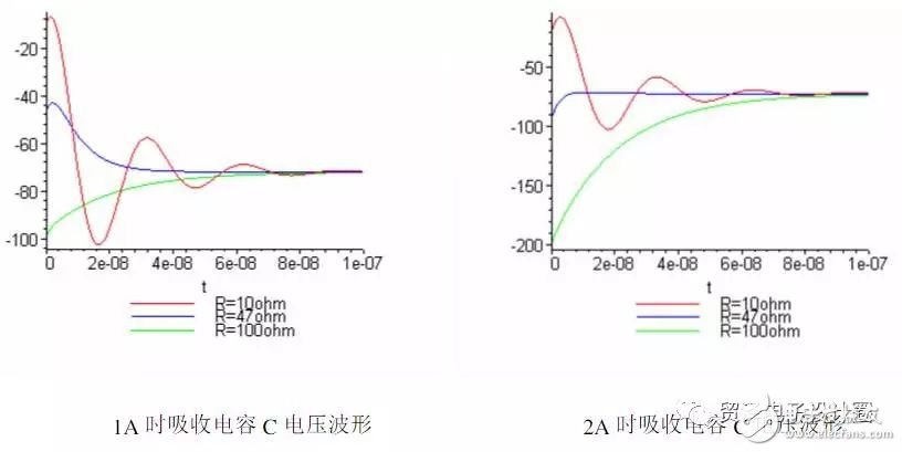
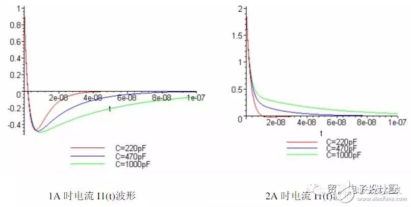
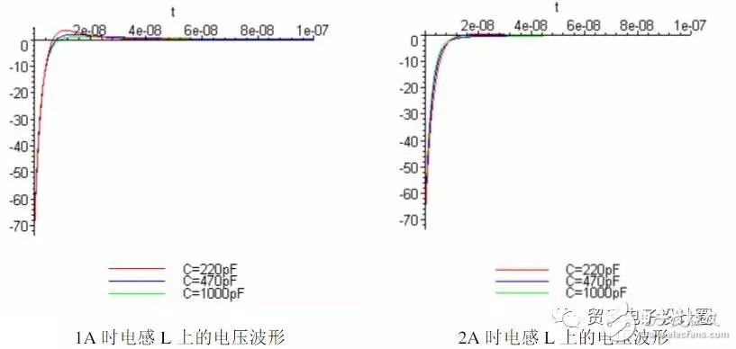
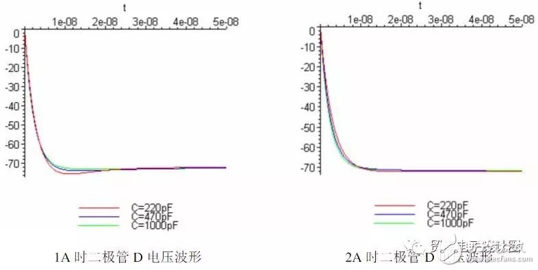
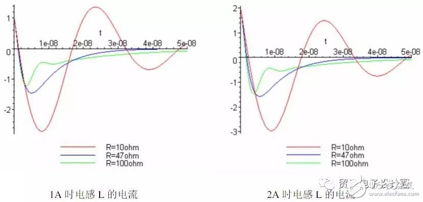
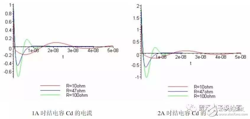
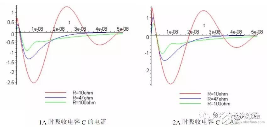
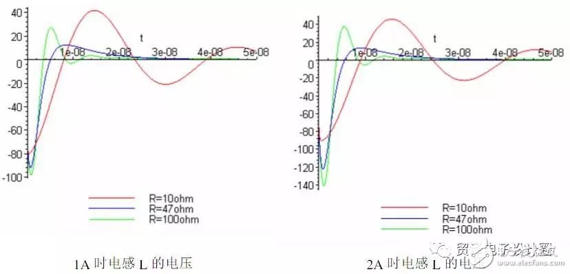
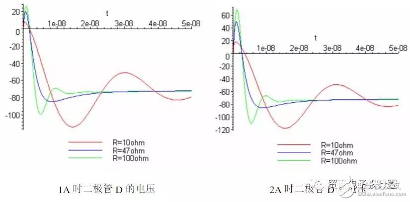
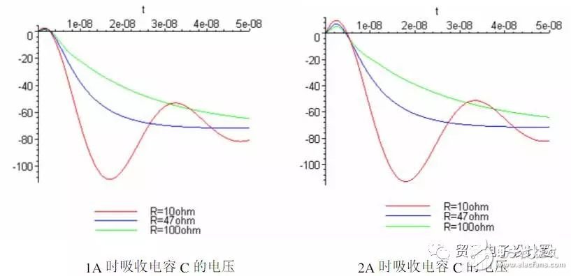
Consider setting Io=1A and 2A in the CCM state.
The effect of different R values ​​on the waveform at C=220pF:
The effect of different C values ​​on the waveform at R=47 ohm:
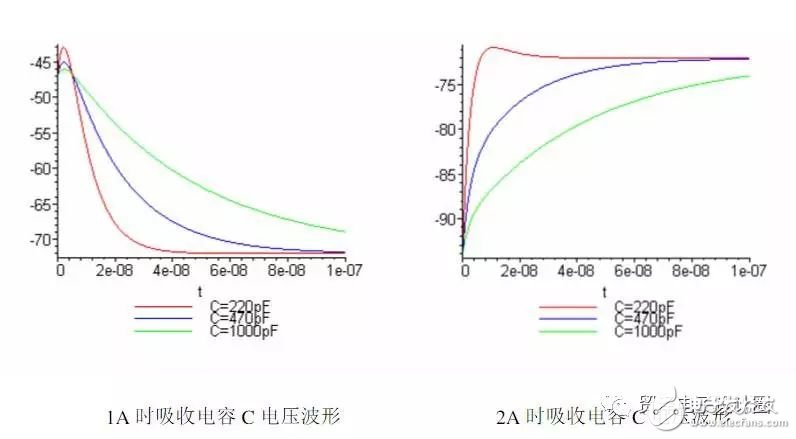
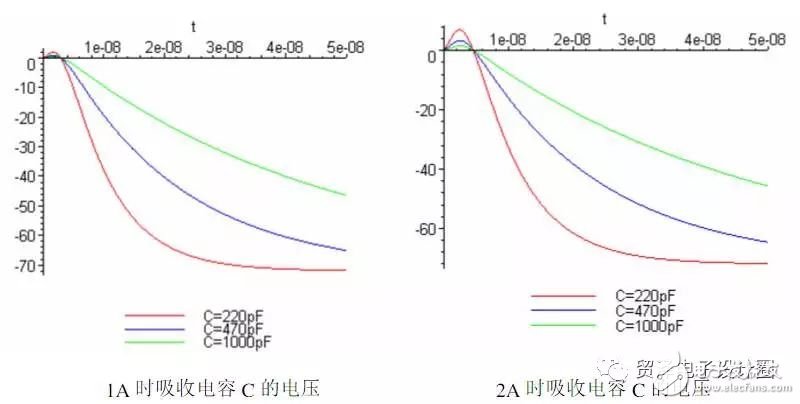
It can be seen that when the off current is relatively large, the larger the resistance, the slower the current drop, the higher the initial voltage on the snubber capacitor, and the higher the voltage withstand voltage requirement. At this time, the voltage across the inductor L and the diode D also changes. It will be faster and will have a greater chance of adversely affecting the loop, so the absorption resistor R should not be too large.
The initial voltage is present on the snubber capacitor because the voltage at both ends cannot be abruptly changed when the diode is turned off, and the inductor L current cannot be abruptly changed, so that the current generates an initial voltage across the snubber capacitor through the snubber resistor.
An increase in the absorption capacitance can reduce the rate of change of the voltage and current.
Consider the power consumed by the absorption resistor R at this time:
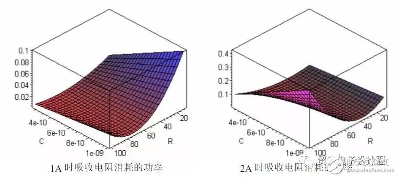
It can be seen that the absorption power always increases with the increase of the absorption capacitor C value, but the different off currents will vary with the change of the absorption resistance R value.
Therefore, an appropriate C value can be selected according to the EMI condition, and then the R value is determined by the C value.
A method of determining the R and C values ​​can be considered. The initial voltage on the absorption capacitor C is determined in the case of the maximum off current. At this time, the R value can be calculated, and the R value is the maximum value, and then calculated by the R value. The C value is obtained, and the C value at this time is the minimum value of the absorption capacitance.
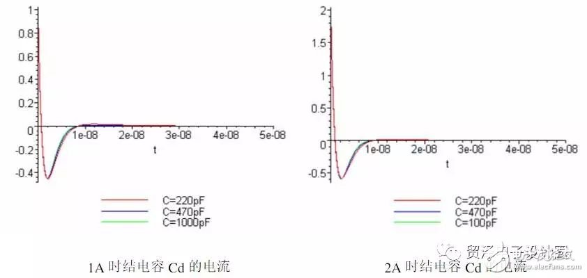
Considering the influence of the junction diode capacitance Cd, let Cd=15pF: DCM state: Io=0,
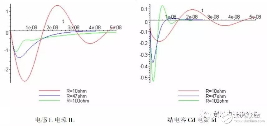

The above are different absorption resistors R, considering different absorption capacitors C:
It can be seen that if the absorption resistance R is too large, the current flowing through the junction capacitance will also increase, and the oscillation will be more severe, which will adversely affect the diode D and will not function as a protection diode.
The increase in the absorption capacitance C can reduce the rate of change of the voltage and current.
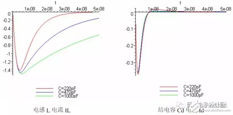
Considering the CCM state, Io is 1A, 2A: C=220pF, the effect of different R:
The effect of different C on R=47 ohm:
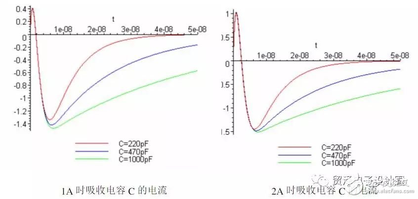
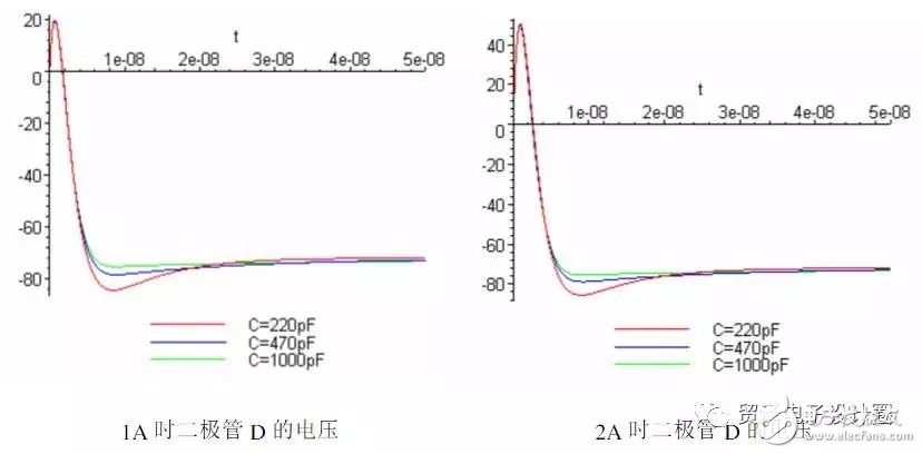
It can be seen that the larger the off current, the higher the peak voltage generated across the diode, the larger the absorption capacitance, the smaller the voltage current change rate, the larger the absorption resistance, and the higher the voltage spike.
The above curve is obtained under the condition that the initial state I(0)=Io, I'(0)=(Vin-Vo)/L, I''(0)= -Io/Cd/L, which is different. The initial conditions will give a different curve. Since the initial conditions are not necessarily correct, the resulting curve may be significantly different from the actual observed waveform, but the trend is for reference.
Bushing Cover For Surge Arrester
Lightning arrester protection box is made of silicone rubber, heat shrinkable material and anti-aging polymer insulation material.
It can effectively prevent all kinds of exposed joints, power failure, damage to electric equipment and electric shock caused by the same short circuit or grounding caused by various factors (wet flash, dirt, contact, small animals or sundry wiring, etc.).
Thus ensuring the power equipment storage.
Applications:
Provide
insulation and protection for surger arrester.
Features:
1.Suitable for 1-35KV.
2.Radiation cross linking materials (Polyolefin or EPDM rubber ).
3.Quick and easy installation.
4.Avoid short circuit and leakage.
5.Facilitate routine inspection and maintenance.
6.Resistant to moisture and dust.
7.Meet RoHS Stand.
8.Customized.
If you want to know more information about our Insulating Tape products, please visit our website.
Bushing Cover For Surge Arrester,Bushing Connection Arrester Cover,Surge Arrester In Transformer,Bushing Cover For Transformer Incoming And Outgoing Feeder
CAS Applied Chemistry Materials Co.,Ltd. , https://www.casac1997.com