
In the industrial field, it is often necessary to use a low-frequency digital phase meter to accurately measure the phase difference between two signals. For example, the power system, frequency characteristics, and laser ranging are widely used. The accuracy of phase detection is directly Determine the overall performance of the system. This requires the measuring instrument to gradually develop in the direction of intelligence and test automation. This design adopts a system scheme that combines MCU and FPGA, taking AVR microcontroller ATmega128 and Altera's Cyclone series EP1C3T100 as the core, giving full play to their respective advantages, such as AVR microcontrollers. With advanced RISC architecture and powerful computing and control functions, Altera's FPGAs are fast, resource-rich and easy to program. With reasonable design, this phase meter has the advantages of high speed, stability and reliability, high precision, and easy implementation. "Intelligent" and "Automation."
1 system design
1.1 Comparison and Selection of Measurement Methods
There are two main methods for phase measurement:
1) The DFT phase detection method is to get the signal to be measured by A/D conversion to get f(n), f(n) is obtained by discrete Fourier transform and the discrete spectrum F(k) is obtained. f(n) and F(k) are The Fourier transform pair obtains the fundamental phase of the two signals through the operation to calculate the phase difference. The accuracy of the DFT phase detection method is limited by the sampling accuracy of the ADC. It requires a high-speed ADC to oversample the signal, and the measurement scheme is complex. The virtual instrument can be implemented on the computer through the acquisition card. Therefore, the application is mainly applied in high-precision applications and virtual environments. Instrument.
2) Filled-counting phase measurement means that two sinusoidal signals with the same frequency get the square wave signal after passing through the signal shaping circuit. After the square wave signal passes the phase detector, two phase difference signals of the input signal are obtained, and the sampling pulse with a fixed frequency is used. Fill and count to calculate the phase difference. Filled-count phasing method is mainly used in applications requiring a certain degree of accuracy, where the measured frequency is not too high but the real-time requirement is very strong. It is easy to realize digitization and automation. The low-frequency digital phase meter is suitable for the fill-count method.
The basic algorithm of the fill-counting phase detection method: if the sine wave shaped square wave signal frequency is f, the period is T, the sampling pulse period is TC, the square wave counts the sampling pulse in one cycle, and n is the measured signal frequency f =1/T=1/NTC. The same method measures the time difference between the two starting points of the same frequency sine wave as Δt, then the phase difference of the two signals Δθ=Δt·360°/T.
1.2 Determination of system plan
According to the system measurement method, the data needs to be acquired, calculated, and displayed. Considering the high integration level of the Programmable Gate Array (FPGA), the richness of the I/O resources, and the stability and reliability, the choice is large, there are few external components, and the price declines in recent years. The advantages, as well as the MCU's good man-machine interface and operation control functions, so the system combines the MCU and FPGA to form the main body of measurement and control. The FPGA is responsible for acquiring pulse signals for frequency measurement and phase difference measurement. The MCU is responsible for reading the data collected by the FPGA and calculating the frequency and phase difference of the signal to be measured and displaying it on the LCD.
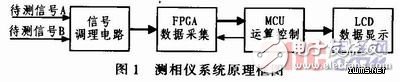
Therefore, the system consists of four parts: signal conditioning circuit to be tested, FPGA data acquisition circuit, MCU data operation control circuit and LCD data display circuit, as shown in Figure 1.
2 Analysis and elimination of measurement errors
The perfect design of the phase measurement instrument not only needs a suitable measurement method and system implementation plan, but also needs to analyze the cause of the error and determine the elimination method.
1) The influence of the filling clock frequency (ie, the data sampling signal) and the determination of the frequency measuring range of this phase measuring instrument is 20 Hz to 20 kHz, and the phase difference range is Δθ=0° to 359.9°. The display of the phase difference is With a resolution of 0.1°, the absolute error of the measured phase is ≤2.
If the measured frequency is 20 Hz ≤ f ≤ 20 kHz, the period is 50μs ≤ T ≤ 50 ms.
T=50 μs, absolute error is 0.1° to 2°.
Fill the clock signal cycle: 0.1° x 50 μs / 360° ≤ TC ≤ 2° x 50 μs / 360 ° ie: 1/72 (μs) ≤ TC ≤ 1/3.6 (μs), the filling clock frequency can be obtained:
3.6 MHz ≤ fC ≤ 72 MHz.
In T=50 ms, the filling pulse count of TC=1/3.6(μs) is counted, the count value Nmin=180000≤218; and the filling pulse count of TC=1/72(μs), the count value Nmax=3600000≤222.
This design considers the MCU's calculation and frequency acquisition to facilitate the signal, fill the clock signal frequency fC = 20 MHz, measuring the absolute error "1 °, FPGA under the effect of 20 MHz clock signal to be measured signal cycle and phase corresponding time difference, FPGA sampling binary data bit is 20 bit, which can ensure the accuracy of measurement.
2) The influence of zero drift in the signal conditioning circuit to be tested and elimination of the signal conditioning circuit The main function of the signal conditioning circuit is to transform the input signal into a rectangular wave, usually using a zero-crossing comparator or a Schmitt trigger.
The zero-crossing comparator may oscillate near the zero point potential. When the input signal is near the zero point potential, the voltage comparator is in the amplification area, and the shaped rectangular wave will generate jitter on the edge, which makes the system unable to measure. To eliminate this jitter, Schmitt triggers can be used. To ensure the accuracy of the measurement, the Schmitt trigger must meet two conditions: one is that the amplitudes of the two signals being measured are substantially equal, and the other is that the threshold level is basically similar.
3) The influence of the steepness of the edge of the shaping edge behind the shaping and the rectangular pulse signal output after the shaping signal is shaped and sent directly to the FPGA, then the FPGA cannot immediately obtain a stable digital pulse signal, which will greatly affect the accuracy of the system. This is mainly due to the fact that the edge of the plastic rear edge is not steep enough. To solve this problem, one is to select a device with a larger slew rate, and the other is to add a differential circuit at the back of the comparator to boost the edge of the pulse signal.
4) The influence of low-frequency measurement accuracy and the elimination of the time difference corresponding to the cycle and phase difference of the 20 MHz data sampling signal to cyclically count the measured signal, with an accuracy of 0.05 μs and a unit of 20 digital quantities of 0.05 μs. Utilize the measured signal to refresh the sampling count, achieve high-frequency multi-measurement, low-frequency measurement, accurate and reliable time counting, so that FPGA can provide stable data for the MCU.
3 system hardware circuit design
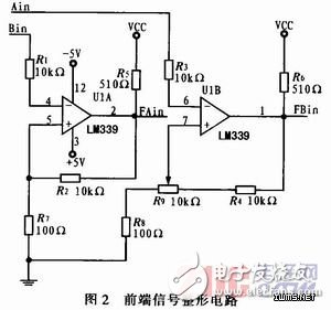
3.1 Design of front-end signal conditioning circuit
Schmitt trigger (hysteresis comparator) can eliminate the jitter caused by comparator zero crossing, but there is a phase difference between the output signal and the input signal if the amplitudes of the two signals under test are substantially equal and two are used. Since the threshold level of the special flip-flop is very close, the phase error introduced by the Schmitt trigger has little effect on the measurement system error.
There are four independent voltage comparators in the LM339. The features of the voltage comparator are: small offset voltage, typically 2 mV; wide supply voltage range, dual supply voltages of ±1 to ±18 V; for comparison signal sources The internal resistance is relatively limited. The difference between the voltages of the non-inverting and inverting inputs is greater than 10 mV to ensure that the output can be reliably switched from one state to another. The output is equivalent to a transistor that does not have a collector resistance. When used, the output is The positive power supply must be connected to a resistor. The interference near the trip voltage value does not exceed the hysteresis AU, and the output voltage value will be stable. Positive feedback can speed up the comparator's response. Because the positive feedback of the hysteresis comparator is very strong and much stronger than the parasitic coupling in the circuit, the self-oscillation caused by the parasitic coupling of the circuit can be avoided. By adjusting the potentiometer, the threshold levels of the two Schmitt triggers are substantially equal, so as to ensure that the input circuit does not bring any error to the phase difference measurement. The circuit is shown in Figure 2.
3.2 System Measurement Circuit Design
The phase meter is designed with the MCU as the core. If the crystal oscillator is 24 MHz, the counting error of the MCU C/T is ±0.5 μs for one machine cycle, the absolute error is 360° x 0.5 μs/50 μs = 3.6°. Therefore, it is difficult to meet the measurement requirements when the frequency of the signal to be measured is high.
This design uses AVR microcontroller and FPGA combination of the program, FPGA to achieve data acquisition, the measured signal frequency and phase difference corresponding time difference is converted to binary data transmitted to the microcontroller; microcontroller to obtain data from the FPGA, after calculation, conversion and other data processing The frequency and phase difference of the signal under test are displayed on the LCD.
System electrical schematic shown in Figure 3. The MCU adopts ATMEL's AVR microcontroller ATmega128, which has an advanced RISC architecture. Most of the instructions are completed in one clock cycle. There are 32 8-bit general-purpose working registers and peripheral control registers, which overcomes the single-chip single-cascade data processing The bottleneck. 128 KB of in-system programmable Flash, 4 KB of EEPROM, and 4 KB of internal SRAM, follow the JTAG standard boundary scan feature, support for extended on-chip debugging, Flash, EEPROM, and fuses are available through the JTAG interface Lock bit programming.
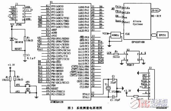
The FPGA adopts EP1C3T100 of ALTEm Cyclone series, the configuration chip is EPCS1, VHDL function program is generated after being totally compiled. SOF and. Pof file, the configuration download is Byte-Blaster II, [Mode] item selects "JTAG" as. The sof file is configured in the FPGA chip EP1C3T100 for debugging; [Mode] item is selected as "AcTIve Serial Programming". The pof file is downloaded to the configuration chip EPCS1, and the system runs normally when it is powered on again.
The LCD uses the HTM12864, a 128x64 serial data transmission LCD monitor, and the backlight is controlled by an optocoupler.
The ATmega128 and EP1C3T100 design their respective JTAG interfaces. Figure 3 depicts the interfaces D0 to D19, EN, Dsel, and LCN of the ATmega128 and EP1C3T100, the RET, D/C, SCLK, and DATA interfaces of the ATmega128 and HTM12864, the input signals FAin and FBin of the EP1C3T100, and a 66 MHz external active crystal oscillator. Configure chip EPCS1.
4 System Software Design
4.1 FPGA Data Acquisition VHDL Programming
FPGA data acquisition VHDL program design is completed on the ALTEra QUARTuslI development software platform and experimental development system. The program design adopts an up-to-down design method. The FPGA system module is shown in Figure 4. The sampling signal generation module completes the frequency division of the clock signal source to obtain CLK=20 MHz; the signal sampling module of the signal to be measured outputs the period of the signal to be measured under the action of the cycle gate signal Tk and the time clear signal Tcr of the control signal generation module. Phase difference data; The measurement data extraction module outputs the cycle and phase difference data under the control of the phase detection signal JXc and the count extraction signal Lad under the control of the output enable signal EN and the data type signal Dsel, and is presented to the MCU operation processing display.
A TPU Screen Protector made of the super toughness of the honeycomb structure. Its unique ultra-soft properties allow it to cover the most complex curves and contours in a device.
The self-healing design of the Hydrogel Screen Protector can protect the display screen of the device from damage, leave no air bubbles, and maintain the sensitivity of the touch screen. Advanced anti-fingerprint and dust- and oleophobic overlays keep your screen smudge- and dirt-free. This overlay is also important in providing maximum touch sensitivity for improved high-speed glide and optimal touch response.
The optical transparency of the Hydrogel Film is more than 90%, showing you the most original screen color and bringing the most realistic visual experience.
If you want to know more about the product information of the Hydrogel Screen Protector for Samsung, please click the product details to view the parameters, model, picture, price and other information of the Samsung Screen Protector.
Whether you are a group or an individual, we will do our best to provide you with accurate and comprehensive information about Hydrogel Screen Protectors!
Screen Protector For Samsung,Hydrogel Screen Protector for Samsung,TPU Screen Protector for Samsung,Hydrogel Film for Samsung
Shenzhen Jianjiantong Technology Co., Ltd. , https://www.tpuscreenprotector.com