
With the rapid development of FPGA technology, Programmable System-on-Chip (SOPC), as a special embedded microprocessor system, combines the advantages of SoC and FPGA, and has hardware and software programmable, scalable, and scalable. The upgradeable features have gradually become an emerging technology direction. The core of SOPC is the embedded microprocessor core implemented on the FPGA. Currently, there are mainly 32-bit soft-core MicroBlaze[1] integrated by Xilinx, 32-bit PowerPC series processor hard core PowerPC405, PowerPC440, ARM CortexA9, and Altera. The company's Nios series of microprocessor soft core and so on. This paper mainly introduces the MicroBlaze soft core structure of Xilinx, introduces its architecture, design flow and related development tools, and adopts this scheme in the actual radio monitoring system [2] to build a miniaturization and intelligence. , networked software radio processing platform.
1 MicroBlaze processor structure The MicroBlaze soft core processor is a configurable Reduced Instruction Set (RISC) 32-bit CPU optimized for Xilinx FPGA chips. Designers can customize the optional configuration of the processor according to the design, depending on the version, configure different options. The soft core processor has the following features:
â—† 32 32-bit general-purpose registers;
â—† 32-bit three-operand instruction word, the instruction word has two addressing modes;
â—† Separate 32-bit address bus and data bus;
â—† High-speed instruction and data buffer, 3-level and 5-stage pipeline operation;
â—† Flexible bus structure, support LMB, OPB, PLB, XCL, FSL on-chip bus interface, etc., the new series also supports AXI bus interface;
â—† Support MMU storage management, FPU floating point unit, cache, exception handling and debugging logic, etc., which can be arbitrarily reduced according to performance requirements and logical area cost.
These features of MicroBlaze greatly expand the scope of application, the core of MicroBlaze processor is still being updated, the current version of MicroBlaze v7.1, its internal architecture is shown in Figure 1.
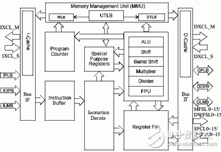
Figure 1 MicroBlaze processor structure
The external interface of the MicroBlaze processor in Figure 1 is defined as follows:
1 DPLB (Data Processor Local Bus), DOPB (Data Onchip Peripheral Bus): Data interface, processor local bus, used for processor and on-chip device data exchange.
2 IPLB (InstrucTIon Processor Local Bus), IOPB (InstrucTIon OnChip Peripheral Bus): Instruction interface for command read channel.
3 DLMB (Data Local Memory Bus): Data interface, local memory bus, for high-speed data exchange.
4 ILMB (InstrucTIon Local Memory Bus): Instruction interface for high-speed instruction reading.
5 MFSL0~15 (Main Fast Simple Link): FSL master device data interface, providing point-to-point data channel; SFSL0~15 (Slave Fast Simple Link): FSL slave device point-to-point data interface.
6 DWFSL0~15: FSL master device directly connects to the interface; DRFSL0~15: FSL slave device directly connects to the interface;
7 IXCL (InstrucTIon side Xilinx CacheLink interface) and DXCL (Data side Xilinx CacheLink interface): instruction cache interface and data cache interface, respectively.
Xilinx's Embedded Development Kit tool EDK [3] (Embedded Development Kit) provides a good tool platform for developing SOPC systems based on MicroBlaze soft core and PowerPC hard processor. Xilinx's EDK tools include: Xilinx Platform Studio (XPS) human machine interface, embedded system tool suite, embedded processing IP core, Platform Studio SDK (Software Development Kit, SDK). XPS provides the following features:
â—† Ability to add cores, edit kernel parameters, perform bus and signal connections, and generate MHS files;
â—† Ability to generate and modify MSS files;
â—† Support all the tools underlying Xilinx;
â—† Ability to generate and observe system block diagrams and design reports;
â—† Multi-user software application support;
â—† Project management;
â—† Process and tool flow depend on management.
A complete embedded processor system design typically consists of three parts: hardware system construction, software system and memory mapping, and application development.
The hardware system is built by the designer to use the Xilinx technology to build a flexible embedded processing subsystem according to the needs of the application. The hardware platform consists of one or more processors or peripherals connected to the processor bus. EDK records hardware platform information through Microprocessor Hardware Specification (MHS) files.
Software systems and memory maps are composed of software drivers and operating systems used to build applications. The created software image file contains only a subset of Xilinx libraries used by the user. EDK records software platform information through the Microprocessor Software Spectifcation (MSS). Designers can run multiple applications on the software platform.
The MHS and MSS data files define the embedded system, and the development process is shown in Figure 2.
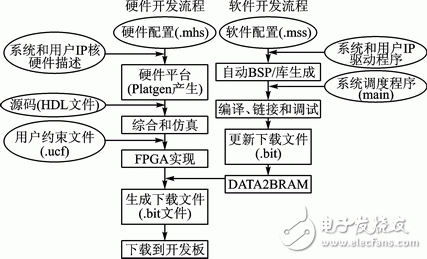
Figure 2 EDK embedded system software and hardware development process
The main function of the safety barrier is to restrict the dangerous energy in the safe place from entering the dangerous place, that is, to limit the voltage and current sent to the dangerous place.
1. Due to the tripartite isolation mode, there is no need for system grounding line, which brings great convenience to the design and on-site construction. The requirements for instruments in hazardous areas are greatly reduced, and isolated instruments are not required on site.
2. Since the signal line does not need to be grounded together, the stability and anti-interference ability of the detection and control circuit signal are greatly enhanced, so as to improve the reliability of the whole system.
3. The isolated safety barrier has stronger input signal processing ability and can accept and process thermocouple, thermal resistance, frequency and other signals, which is impossible for Zener safety barrier.
4. The isolated safety barrier [2] can output two mutually isolated signals to be used by two equipment using the same signal source, ensure that the signals of the two equipment do not interfere with each other, and improve the electrical safety insulation performance between the connected equipment.
Isolated Safety Barrier,Output Intrinsic Isolated Safety Barrier,Explosion-Proof Relay Isolated Barrier,Switch Explosion-Proof Relay Barrier
Taizhou Jiabo Instrument Technology Co., Ltd. , https://www.taizhoujiabo.com