
Over the past 30 years, MEMS switches have been recognized as a superior replacement for electromechanical relays with limited performance. The ease of use and the ability to reliably perform small switches from 0 Hz/dc to hundreds of GHz with minimal loss have revolutionized the way electronic systems are implemented.
This performance advantage can impact a large number of device types and applications. Through MEMS switching technology, electronic measurement systems, defense system applications, and health care equipment can achieve levels of performance and appearance that were previously difficult to achieve.
Establish a huge product business
Modern switching technology has its drawbacks, so no single technology can be the ideal solution. Disadvantages of relays include narrow bandwidth, limited actuation life, limited channel count, and large package sizes. Compared to relays, MEMS technology has the potential to provide world-class RF switching performance and an order of magnitude improvement in reliability in small form factors.
Many companies that are trying to develop MEMS switching technology are already investing in reliable product production, but this challenge is hindered. One of the first companies to enter the MEMS switch research was Foxboro, which in 1984 submitted the world's first electromechanical MEMS switch patent. ADI has been involved in the study of MEMES switching technology in early academic projects since 1990; in 1998, ADI has developed MEMS switch designs for early prototypes; and in 2011, ADI for its MEMS switch program A substantial investment has been made, which has led to the construction of ADI's own state-of-the-art MEMS switch manufacturing facilities.
Now, ADI has the ability to provide the industry's "productionable", "highly reliable", "high performance", "small form factor" MEMS switches to replace the outdated relay technology.
ADI has a wealth of experience in MEMS. ADI's first successful development, production, and commercial MEMS accelerometer products were published in 1991 as the ADXL50 accelerometer; ADI released the first integrated MEMS gyroscope-ADXRS150 in 2002. Starting with this, ADI has built a huge MEMS product business and an unparalleled reputation to produce reliable, high-performance MEMS products. ADI has produced more than one billion inertial sensors for automotive, industrial and consumer applications. It is such a lineage that brings experience and trust to drive the realization of MEMS switching technology.
The basis of MEMS switches
At the heart of ADI's MEMS switching technology is the concept of electrostatically actuated, cantilevered beam switch assemblies. In essence, it can be thought of as a micron-scale mechanical relay with metal-to-metal contacts that can be electrostatically actuated.
The switch is linked in the configuration settings of the three groups of terminals. Functionally, a terminal can be considered a source, a gate, a bungee, and the like. A simplified graphical representation of the switch for the A condition is shown in Figure 1, showing that the switch is in the closed position. When the dc voltage is applied to the gate, a pull-down force of static electricity is generated at the switch beam.
The same electrostatic pull down force can be seen in parallel plate capacitors with positive and negative charge plates that will attract each other. When the gate voltage is increased to a high enough value, it produces enough attractive force (red arrow) to overcome the resistance spring force of the switch beam, and the switch beam begins to move down until the contact touches the drain. This condition is shown in the B condition in Figure 1. This completes the circuit between the source and the drain, and the switch is now turned on. The actual force required to pull the switch beam down is related to the spring constant of the cantilever beam and its resistance to movement.
Please note that even in the open position, the switch beam will still have a spring force (blue arrow) that pulls the switch up, but as long as the electrostatic force pulled down is relatively large, the switch will remain open. Finally, when the gate voltage is removed (C condition in Figure 1), that is, 0 V on the gate electrode, the electrostatic attraction will also disappear, and the switch beam will have sufficient restoring force (blue arrow). The spring acts to open the link between the source and the drain and then return to the original closed position.
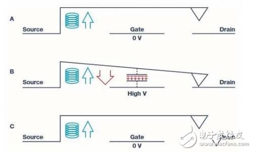
Figure 1: MEMS switch actuation program, A and C for switch off, B for open
The four main steps in manufacturing a switch using MEMS technology are shown in Figure 2. The switch is constructed of a high resistivity silicon chip with a thick dielectric layer deposited on top to provide superior electrical isolation from the underlying substrate. Internal links to MEMS switches are implemented using a standard back-end CMOS internal link process. Both low-resistivity metals and polysilicon are used to make electrical links to MEMS switches and are embedded in the dielectric layer.
Metal vias, indicated in red, are used to provide a link to the switch inputs and outputs, as well as to provide gate electrodes to any of the locations in the chip. The cantilever MEMS switch itself is surface micromachined using a sacrificial layer to create an air gap below the cantilever beam. The cantilever switch beam structure and bond pads are made of gold. Both the switch contacts and the gate electrodes are made of a thin metal of low resistance and are deposited on the surface of the dielectric.
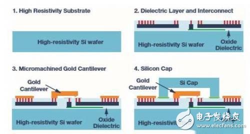
Figure 2: Overview of MEMS Switch Manufacturing
The wire bond pads are also constructed using the steps described above. Gold wire bonding is used to link the MEMS chip to the metal lead frame and package it into a plastic four-sided flat pinless (QFN) chip, making it easy for the surface to adhere to the PCB. The chip is not limited by any type of packaging technology. This is because a high resistivity silicon cap is bonded to the MEMS chip and a sealed protective casing is formed on the periphery of the MEMS switch assembly. Sealing the switch in this way can improve the environmental tolerance and cycle life of the switch, regardless of the external packaging technology used.
Figure 3 shows four sets of MEMS switches in a single-pole, four-throw (SP4T) multiplier configuration setting. Each set of switch beams has five sets of parallel ohmic contacts to reduce resistance and improve power handling when the switch is closed.

Figure 3: Close-up graphics showing four sets of cantilever switch beams (SP4T configuration settings)
As mentioned at the outset, MEMS switches require a high dc drive voltage to electrostatically actuate the switch. In order to make the parts as easy to use as possible and to further ensure their performance, ADI has designed a matching driver IC to generate high dc voltage and is packaged in a QFN together with the MEMS switch.
In addition, the resulting high actuation voltage is applied to the gate electrode of the switch in a controlled manner. It will increment to a high voltage on the microsecond time scale. The incremental approach helps to control how the switch beam is attracted and pulled down, and improves the actuation, reliability, and cycle life of the switch.
Figure 4 shows the driver IC and MEMS chip in situ in the QFN package. The driver IC requires only low voltage, low current supply and is compatible with standard CMOS logic drive voltages. This co-packaged drive makes the switch very easy to use and has very low power requirements: in the 10 mW to 20 mW area.
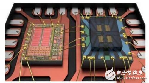
Figure 4: Driver IC (left side), MEMS switch chip (right side) is glued and wire bonded to the metal lead frame
MEMS switch reliability
The key principle of any new technology is how reliable it is, and ADI is very clear. The new MEMS technology manufacturing process is the foundation for the development of robust, high-performance switch designs. This combination of a sealed silicon-clad process is critical to providing a reliable long-lasting MEMS switch.
In order to successfully commercialize MEMS switches, extensive reliability testing is required for MEMS, such as switching operation cycles, life tests, and mechanical vibration tests. In addition to this test, and in order to ensure the highest possible quality, the parts have been verified by a full range of standard IC reliability tests.
In RF instrumentation applications, a sufficiently long switch actuation life is of paramount importance. Compared to electromechanical relays, the development of MEMS technology has brought an order of magnitude improvement in cycle life. The high temperature operating life (HTOL I) test and the early failure (ELF) qualification test at 85 °C can strictly guarantee the cycle life of the part.
Continuous on-life (COL) performance is another key parameter in MEMS switching technology. For example, the way the RF instrument switch can be used can change, and the switch can have more time to stay on. ADI has recognized this fact and is committed to achieving superior COL life performance for MEMS switching technology to mitigate life risk. From the initial 7-year COL life performance level at 50 °C, ADI has further developed a technology that provides leading-edge products with a 10-year COL at 85 °C.
MEMS switch technology has undergone a complete set of mechanical durability certification tests. A total of five tests are listed in Table 1 to ensure the mechanical durability of the MEMS switch. Due to the small size and low inertia of the MEMS switch assembly, it is significantly more durable than electromechanical relays.
Strong performance advantage
The key strength of the MEMS switch is its ability to provide 0 Hz/dc precision and wideband RF performance with excellent reliability vs. relays on a small surface mount form factor.
One of the most important quality factors of any switching technique is the on-resistance of a single switch multiplied by the off capacitance. This is often referred to as the RonCoff coefficient and is expressed in femtoseconds. When RonCoff drops, the insertion loss of the switch is also reduced, and the off isolation is improved. For a single switching unit, the ADI MEMS switching technology has a RonCoff factor of less than 8, which will ensure its position as a technology choice for world-class switching performance.
This basic advantage can be used to achieve superior RF performance levels with a discreet design. Figure 5 shows the insertion loss and turn-off isolation for a prototype QFN, single pole double throw (SPDT) MEMS switch. The insertion loss is only 1 dB at 26.5 GHz and a bandwidth of more than 32 GHz has been achieved in the QFN package.
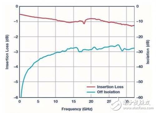
Figure 5: SPDT MEMS Switch Performance in QFN Package
Figure 6 shows a larger frequency sweep from prototype insertion loss and turn-off isolation in the probing of a single-pole double-throw (SPST) switch. At 40 GHz, 1 dB insertion loss can be achieved with off-isolation in the – 30 dB region.
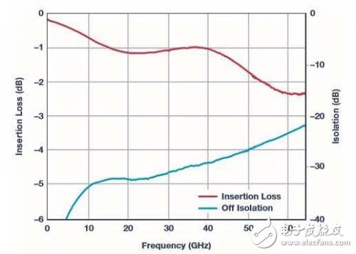
Figure 6: SPST MEMS switch performance under bare chip probing
In addition, the design of the MEMS switch itself can provide very high performance in the following areas:
**Precise dc performance: less than 2 Ω RON, 0.5 nA turn-off leakage, and –110 dBc total harmonic distortion (THD + N) precision performance levels have been achieved with improved beam and substrate optimization The potential of all levels.
** Linearity performance: The third-order intercept point (IP3) level above 69 dBm is implemented with an input tone of 27 dBm. There is also the potential to increase by more than 75 dBm throughout the operating frequency band.
**Acoustic life: Guaranteed a minimum of 1 billion actuation cycles. This has far exceeded the mechanical relays on the market today - the general rating is less than 10 million cycles.
**Power Processing (RF /dc): Power supplies over 40 dBm have been tested throughout the operating frequency band and will not degrade at lower or higher frequencies. In terms of dc signals, this switching technology can pass currents above 200 mA.
Finally, solutions with small size are often a key requirement common to all markets. MEMS here again provides a compelling advantage. Figure 7 shows an isometric comparison of the packaged ADI SP4T (four sets of switches) MEMS switch design with a typical DPDT (four sets of switches) electromechanical relays.
In terms of volume, the space savings are quite obvious. In this case the MEMS switch requires only 5% of the relay volume. This very small size can significantly drive board space savings, especially for double-sided board development. This is especially valuable for automotive test equipment manufacturers because higher channel densities are of paramount importance.
Figure 7: ADI MEMS switches (four sets of switches) packaged in leadframe chips compared to typical electromechanical RF relays (four sets of switches)
in conclusion
The MEMS switching technology developed by ADI has made a dramatic leap in switching performance and size reduction. Best performance in its class: from 0 Hz/dc to Ka-band and above, improved cycle life compared to relay orders of magnitude, excellent linearity, very low power requirements, and supply of chip-scale packages, etc. Both make ADI's MEMS switching technology revolutionize new products for ADI's switch portfolio.
Type1 Tethered Cable,16A Type1 Tethered Cable,32A Type1 Tethered Cable,Type 1 Tethered Charging Cable
Yangzhou JERI New Energy Co., Ltd. , https://www.jrevcharging.com