
MAX2170 S11 Data for VHF and L-Band Input Abstract: This applicaTIon note shows how the MAX2170 triple-band (T-DMB, DAB, FM) receiver's input-scattering parameter (S11) is measured for the VHF and L-band inputs. The VHF input consists of a bandpass tracking filter followed by an LNA. The return loss will be good for the desired channel, but will look reflecTIve for the out-of-band channels. As a result, the S11 data will change significantly as the MAX2170 tunes to a new channel. To address this issue, the series 91nH inductor, which is part of the VHF tracking filter, was removed from the input for the S11 measurements (Figure 1). Removing this component changes the tracking filter's shape but allows S11 calibraTIon to the pin of the IC. Note, however, that the 91nH inductor is required for the tracking filter to operate properly. It must be used in the final application. The L-band input consists of ESD diodes and an LNA. The input will look resistive with some shunt capacitance. The S11 data for this input will not vary when the MAX2170 tunes to a new channel. The L-band input can be modeled as a resistor R = 23.4Ω in series with C = 4.2pF. 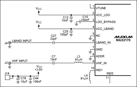 Figure 1. Schematic of the VHF and L-band inputs to the MAX2170. The 91nH inductor for the VHF input can be removed for calibration of S11 data. Performance Summary Table 1 shows S11 data (magnitude and phase) for the VHF and L-band inputs. The RF frequency is changed for each measurement. Table 1. S11 (Magnitude / Phase) for VHF and L-Band Input
Table 2 shows S11 data (real and imaginary) for the VHF and L-band inputs. The RF frequency is changed for each measurement. Table 2. S11 (Real / Imaginary) for VHF and L-Band Inputs
Test Results 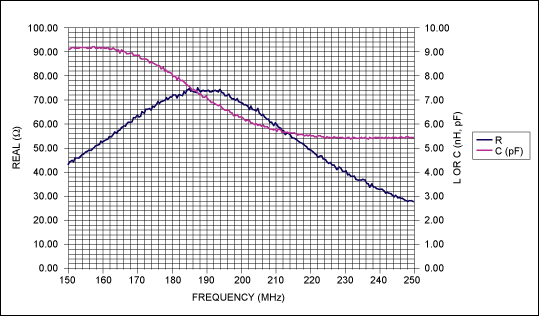 Figure 2. The Thevenin equivalent resistance and capacitance for the VHF input when the RF is tuned to 174.928MHz. 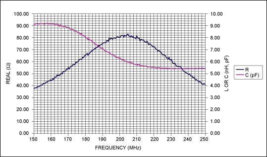 Figure 3. The Thevenin equivalent resistance and capacitance for the VHF input when the RF is tuned to 204.64MHz. 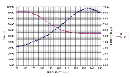 Figure 4. The Thevenin equivalent resistance and capacitance for the VHF input when the RF is tuned to 239.2MHz. 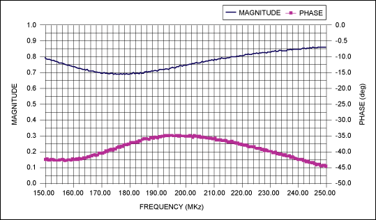 Figure 5. S11 magnitude and phase for the VHF input with the MAX2170 tuned to 174.928MHz. Note that this s-parameter data will change if the MAX2170's RF frequency changes. 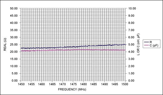 Figure 6. The Thevenin equivalent resistance and capacitance for the L-band input. The Thevenin equivalent circuit looks the same for RF frequencies from 1450MHz to 1500MHz. The average value is R = 23.4Ω in series with C = 4.2pF. 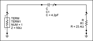 Figure 7. The Thevenin model of L-band RF input in a 50Ω system 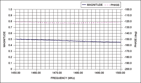 Figure 8. S11 magnitude and phase for the L-band input. Test Files The following test files contain S11 data in CITIFILE format for the MAX2170.
| ||||||||||||||||||||||||||||||||||||||||||||||||||||||||||||||||||||||||||||||||
OEM Laptop Ram manufacturer Memoria Ram ddr 4 4g 2666 memory sodimm 4gb ddr4 2666mhz dual channel RAM for laptop 16c PC4 21300 1Rx8
• 240-pin, unbuffered dual in-line memory module (UDIMM)
Ddr4 Desktop Memory,Ddr3 4Gb 1600Mhz,Ddr3 4Gb Ram Game Memory,Ddr3 8Gb Desktop Memory
MICROBITS TECHNOLOGY LIMITED , https://www.hkmicrobits.com