
1 Product Introduction
The HC89F003 is an enhanced 8-bit microcontroller developed in a high-frequency, low-power CMOS process with 16K Bytes of FLASH program memory, 256 Bytes of IRAM and 256 Bytes of XRAM, 18 bidirectional I/O ports, and 5 16-bit timings. / Counter, 3 groups of 12-bit with dead-band control complementary PWM, 1 8-bit PWM, 2 UARTs, 1 SPI, 16 external interrupts, 8+2 12-bit ADCs, four system operating modes (normal, Low frequency, power down and idle) and 16 interrupt sources.
A lot of interrupts are used on the microcontroller. On this chip is enough to meet most of the product design.
Hc89f003 has:
ï¬ 16 interrupt sources
ï¬ Level 4 interrupt priority
ï¬ 16 external interrupts
The key point is: Generally, our MCUs, such as 51, have less re-mapping functions, such as stm32, and their remapping functions basically have fixed pins. However, hc89f003 is different. Most of his pins can be remapped. For example, P00 can be used as an io port and can be remapped to usart_tx, usart_rx, iic, spi, etc. In other words, when designing the board, you don't have to worry about the hardware connection error. As long as the connection is made, the remapping function can basically be realized.
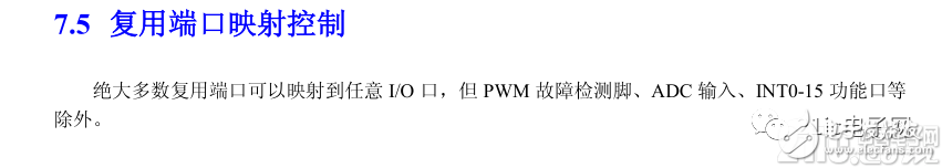
Description given by the Datasheet: Most of the multiplexed ports can be mapped to any I/O port, except for the PWM fault detection pin, ADC input, and INT0-15 function port.
Note that when multiple outputs are mapped to a port, only one output is valid. Port remapping is similar to interrupts and has priority.
*The following are the default priorities:

such as:
CLKO_MAP is configured as 0x01. Select P0.1 port as the output port of CLKO, and T4_MAP is also configured as 0x01. At this time, the hardware will follow the above priority level, P0.1 will be configured as the output port of CLKO, and the configuration of T4_MAP is invalid.
When all port mapping control registers are not equal to 0x01, that is, all function ports do not select P0.1 as the input and output port. At this time, the output of this port is the first bit of the P0 port data register.
Inputs can be configured to enter multiple functions from a PAD pin, such as:
When T0_MAP is configured as 0x23, P2.3 is selected as the input port of T0, and T5_MAP is also configured as 0x23, so that the signal entering from the P2.3 port acts on both T3 and T5.
When both TXD and RXD are configured on one port and this port is set to output, TXD and RXD are internally connected.
At the time of input, the read port data register reads the value on the chip pin regardless of the function of the port.
For questions about the remapping feature, please read the official datasheet carefully. Http://HC89F003_003P_SPEC_Ver1.03.pdf (After all, it is China's core product, the datasheet is not stressful to read. Previously, I used to read English, so that my children who have not passed the fourth grade are big.)
HC89F003 Notes on use: (An important note of the official datasheet, be sure to carefully look at the datasheet when using the chip)
1. To ensure the stability of the system, a capacitor must be connected between VDD and GND (the capacitance must be equal to or greater than 0.1μF). (For this, we usually do this when we use the chip, add a capacitor)
2. To ensure the power-on stability of the system, it is recommended that the client program perform a soft reset operation of the re-read code option after the system generates a POR reset. The official said that this has been improved (I think it is still very OK to go to the official website to download the new version of the datasheet)
3. When using the ADC module, the system operating voltage VDD must be higher than 2.7V regardless of the reference voltage selection. (The reference voltage is generally GND, this vdd is generally 3.3v)
4. External Interrupt When using the polling mode, the interrupt flag bit cannot be cleared normally. The interrupt can be cleared by first disabling the interrupt enable bit, and then enabling the external interrupt to generate a normal external interrupt after the interrupt flag is cleared. There is no such problem when using the interrupt method.
5. When the user selects the port input external clock using the T3 count clock source, the configuration of TR3 and T3CLKS[1:0] should be performed simultaneously (ie, complete the configuration with one instruction). (Personal feelings are strange, but still can be done according to him. He said an instruction is an instruction.)
Introduced so much, it is time to open the box map.
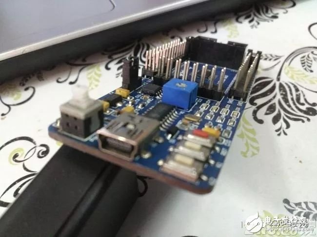
I received the board before the National Day, and I was surprised by the small one. Thanks to the 21ic little speaker, I am happy.
After opening, you can see a development board, a 51link and a data line.
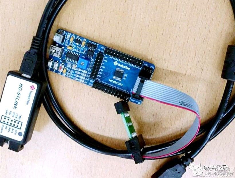
I saw 51-link for the first time, a little surprised. Hahaha, blame me for not enough knowledge. . . . I have to work hard.
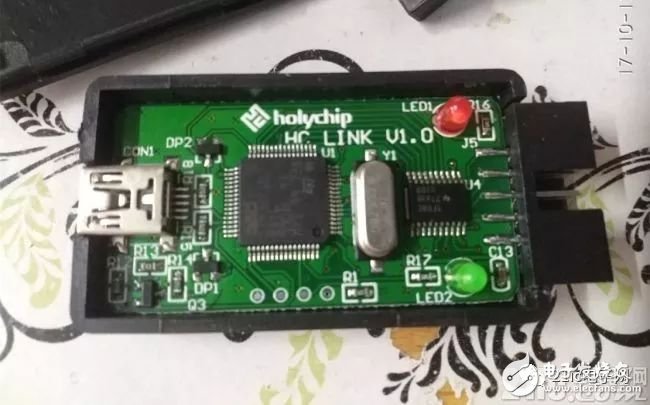
Open to see what is inside 51link, a look, scared, turned out to be stm32f1 series chips.
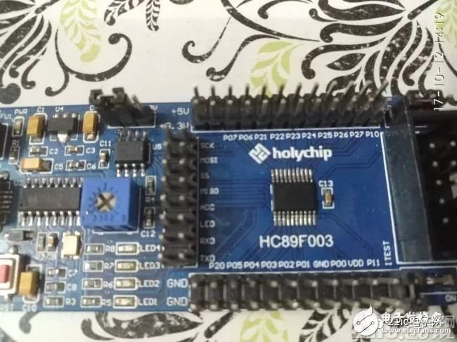
This small board is still very delicate, buttons, and some necessary circuits are mounted on this small piece.
All 20pin io ports have been brought out. Onboard ch340 drive circuit
Then download a bunch of data, open it, not the chip of the 51 core, it is not difficult. (This is the idea I just started... I found out that I was wrong. When I was doing a smart car, I said that when you despised it from the beginning, you have already lost half of it... but it’s ok , I can still get it done haha)
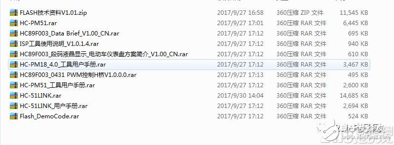
Go to the official website of the core Sheng Electronics to download a bunch of information, slowly look, install the driver, install hc-link, then open the routine code, open the datasheet, and slowly engage. . .
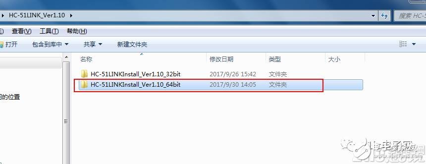
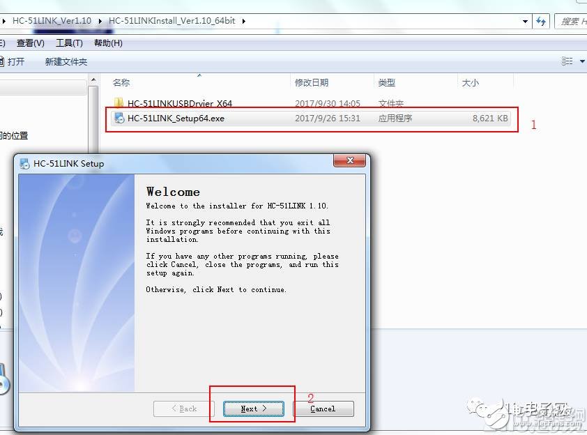
I also downloaded it first, and then installed hc-51link first, this is relatively simple, there are user manuals there.
The explanation of other systems is very detailed. I am 64-bit win7, which is relatively simple.
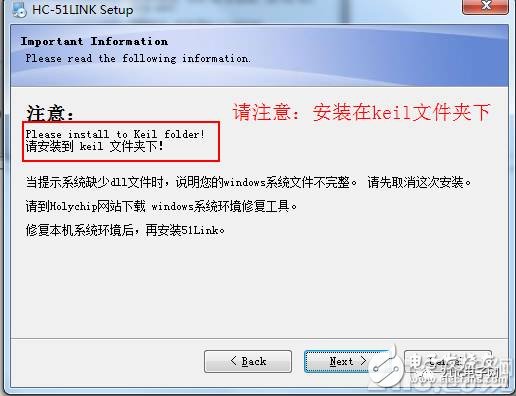
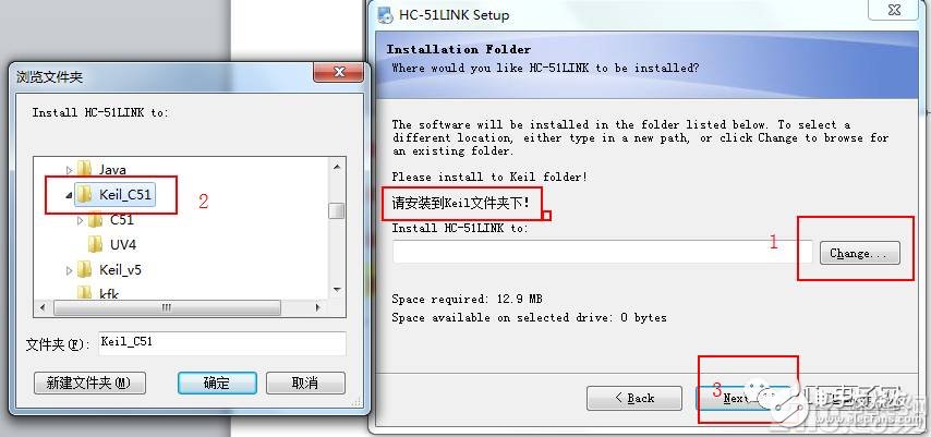
Please note: Installed in the keil folder.
Please note: Installed in the keil folder.
Please note: Installed in the keil folder.
The important thing is to say 3 times.
Then it will be next to the next, it is recommended to remove the anti-virus software from 360 and then install.
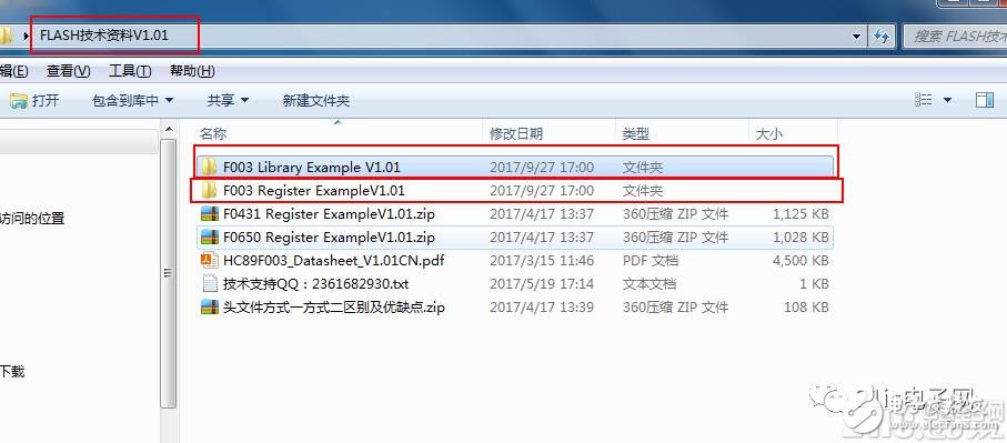
Then open flash technical data > F003 Library Example V1.01
This is a routine for the library function version, much like stm32. Getting started is not difficult to play.
F003 Register ExampleV1.01> This is the register version. I did not see.
Just open a gpio project:
I saw it for the first time, oh, how are you so familiar,,,,,, hahaha
Look into the system initialization, the core part is to choose the system clock
/**
* @Describe the system clock OSC frequency, ie peripheral clock (Timer UART SPI, etc.)
* @Parameter OscClock : OSC clock setting
* CLK_OSC_32MHZ / / system clock 32M
* CLK_OSC_16MHZ / / system clock 16M
* CLK_OSC_8MHZ / / system clock 8M
* CLK_OSC_4MHZ / / system clock 4M
* CLK_OSC_44KHZ / / system clock 44KHZ
* @回值ErrorStatus: indicates the OSC configuration status
* Refer to the ErrorStatus enumeration class.
* @注æ—
*/
ErrorStatus CLK_OscClockConfig(CLK_OscClock_Typedef OscClock)
{
U8 OscClkBuf;
If(OscClock == CLK_OSC_44KHZ)
{//Use low frequency as system clock
CLKSWR = (CLKSWR&(~CLK_SYS_SEL))|CLK_OSC_44KHZ; //Open low frequency crystal
While((CLKSWR&CLK_SYS_STA)!=CLK_RC44KHZ_FLAG);//waiting for crystal oscillator to startReturn SUCCESS;
}
Else
{//Use high frequency as system clock
If((OscClock == CLK_OSC_32MHZ)&&(CLKDIV < CLK_CLKDIV_RESET_VALUE)) return ERROR; / / If the final CPU clock is higher than 20M, the configuration fails
CLKSWR = (CLKSWR&(~CLK_SYS_SEL))|CLK_RC32MHZ; //Start internal high frequency
While((CLKSWR&CLK_SYS_STA)!=CLK_RC32MHZ_FLAG); //waiting for high-frequency crystal oscillator to start
OscClkBuf = CLKDIV;
CLKDIV = 2; // Ensure that the CPU works below 20M.
CLKSWR = OscClock|(CLKSWR&(~CLK_RC32M_DIV)); //Set the RC32M division factor
CLKDIV = OscClkBuf; //Restore CPU division factor
Return SUCCESS;
}
}
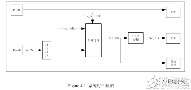
The HC89F003 microcontroller system clock has two clock sources: internal high frequency RC clock (32 MHz) and internal low frequency RC clock (44KHz). Among them, the internal high frequency RC does not exceed 1% in the range of -40 ° C ~ +85 ° C. The selected system clock (if the internal high frequency RC is selected, the clock divided by RC32M_DIV[1:0]) is recorded as osc_clk, the frequency is F osc , and the period is T osc .
Mainly used for peripheral modules, osc_clk can divide the arbitrary value between 1-255. The divided clock is recorded as the CPU clock. The frequency is F cpu and the period is T cpu .
The CPU can run at up to 20MHz. If the selected clock source frequency is higher than 20MHz, it needs to be divided to make the CPU clock frequency equal to or lower than 20MHz.
The clock of the internal low-frequency RC (RC44K) output is recorded as wdt_clk, which is used for the count of the watchdog timer. It can also be used for the system clock. The clock of the internal high-frequency RC (RC32M) output is recorded as rc32m_clk, which can be 1/2/ 4/8 divided.
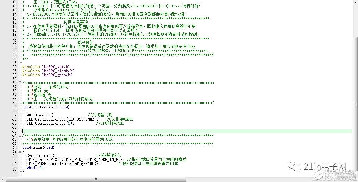
After the system is initialized, the pins of the chip can be operated. . . .
Then there is the initialization function of GPIO. The core is still very good for us. The library function has been integrated, and the direct call is OK.
A code thing:
GPIO_Init( GPIOT0, GPIO_PIN_2, GPIO_MODE_IN_PU ); //Set the P02 port to pull-up resistor mode
The use of library functions is very simple, if I want to set P00 to push-pull output mode. . .
Directly change GPIO_PIN_2 to GPIO_PIN_0 .
GPIO_MODE_IN_PU becomes GPIO_MODE_OUT_PP
GPIO_Init( GPIOT0, GPIO_PIN_0, GPIO_MODE_OUT_PP ); //P00 is set to push-pull output mode
/**
* @Description mode for one or more IOs in a group of ports
* @Parameter GPIOx : Initialized port group (x:0-2)
* GPIOT0 //Port 0 group
* GPIOT1 //Port 1 group
* GPIOT2 //Port 2 group
* @Parameter GPIO_PIN : Initialized port number
* GPIO_PIN_0 //Select port 0
* GPIO_PIN_1 //Select port 1
* GPIO_PIN_2 //Select port 2
* GPIO_PIN_3 //Select port 3
* GPIO_PIN_4 //Select port 4* GPIO_PIN_5 //Select port 5
* GPIO_PIN_6 //Select port 6
* GPIO_PIN_7 //Select port 7
* @Parameter GPIO_Mode : Initialization mode
* GPIO_MODE_IN // digital input
* GPIO_MODE_IN_PD / / with pull-down input
* GPIO_MODE_IN_PU //with pull-up input
* GPIO_MODE_IN_AN / / analog input
* GPIO_MODE_IN_SMT // digital input SMT
* GPIO_MODE_IN_PD_SMT //With pull-down input SMT
* GPIO_MODE_IN_PU_SMT //With pull-up input SMT
* GPIO_MODE_IN_AN_PU_PD / / analog input on the pull-down at the same time, B version after the chip support
* GPIO_MODE_OUT_PP // push-pull output
* GPIO_MODE_OUT_OD // open drain output
* GPIO_MODE_OUT_OD_PU //Open drain with pull-up output
* @return value no
* @注æ—
*/
Void GPIO_Init(GPIO_TypeDef GPIOx, GPIO_Pin_TypeDef GPIO_PIN, GPIO_Mode_TypeDef GPIO_Mode)
{
U8 i;
U8 xdata *gpioset;
Gpioset = 0xFF00 | ((GPIOx - 1)<<3);
For(i=0;i<8;i++){
If((GPIOx == GPIOT1)&&(i>1))break;
If(GPIO_PIN&0x01){
*(gpioset+i/2) = ((*(gpioset+i/2)) & (0xF0 >> ((i%2)*0x04))) | (GPIO_Mode << ((i%2)*0x04) );
}
GPIO_PIN >>= 1;
}
}
The above is the original function of void GPIO_Init (GPIO_TypeDef GPIOx, GPIO_Pin_TypeDef GPIO_PIN, GPIO_Mode_TypeDef GPIO_Mode) . .
If you are interested, you can jump in and have a look. You can do it without looking.
Open HC89F_GPIO.H
Pull down the bottom. Functions with gpio can be called directly.
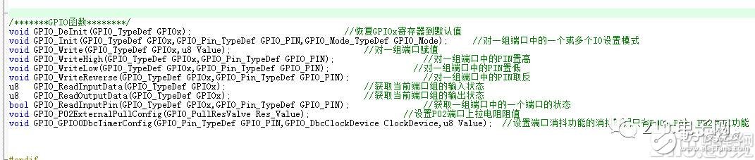
For example, we need to light a led light, call this function:
Void GPIO_Write(GPIO_TypeDef GPIOx, u8 Value); //Assign a set of ports
See the schematic of the board:
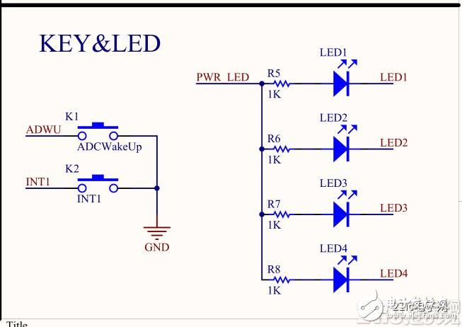
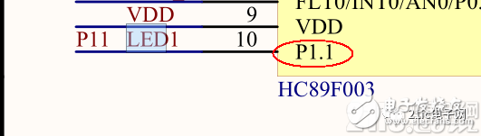
LED1 is connected to the P11 pin of the HC89F003, then we light it up to make the P11 pin low.
Void main(void)
{
System_init (); / / system initialization
GPIO_Init(GPIOT1, GPIO_PIN_1, GPIO_MODE_OUT_PP); //P00 is set to push-pull output mode
GPIO_Write(GPIOT1, 0xFD); //Set P11 pin to low level
While(1);
}
Then download to the microcontroller, the download settings there, written in the HC-51LINK user manual is very detailed.
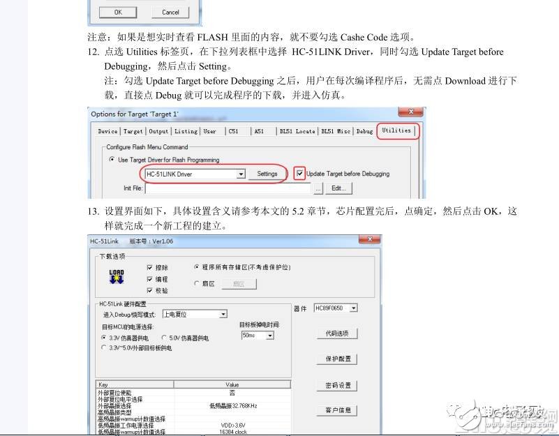
Various configurations have been written. Although it is a bit of a hassle, but the tutorial is very detailed, please be patient and complete the configuration. Xinsheng is a manufacturer that makes products with heart. . .
Also, I found a very special place. This is what I didn't have before playing 32/51. That is, the resistance of the pull-up resistor is optional. The programmable option, the product of Xinsheng once again surprised me.
/**
* @Describe the setting of the pull-up resistor value of P02 port
* @Parameter Res_Value : Resistance value
* R050K // pull-up resistor 50K
* R100K // pull-up resistor 100K
* R150K // pull-up resistor 150K
* R300K // pull-up resistor 300K
* @return value no
* @注æ—
*/
Call this function:
Void GPIO_P02ExternalPullConfig(GPIO_PullResValve Res_Value)
{
P0LPU = (P0LPU&(~GPIO_P02PU))|(Res_Value&GPIO_P02PU);
}
Ex:
Void main(void)
{
System_init (); / / system initialization
GPIO_Init(GPIOT0, GPIO_PIN_2, GPIO_MODE_IN_PU); //Set the P02 port to pull-up resistor mode
GPIO_P02ExternalPullConfig(R100K); //Set the P02 port pull-up resistor to 100K
While(1);
}
You can set the P02 port pull-up resistor to 100K.
Then introduce the remapping function of HC89f003:
Datasheet introduction:
Let's see how to remap, I will try to explain it briefly.
What is remapping:
There are many I/O ports on a typical MCU, and there are many built-in peripherals such as I2C, ADC, ISP, USART, etc. In order to save the pin, these built-in peripherals are basically shared with the I/O port. That is, the multiplexing function of the I/O pins. Many of the I/O pins that multiplex the built-in peripherals can be pulled out from different I/O pins through the remapping function, that is, the pins of the alternate function can be changed programmatically. I understand that everyone should understand some of the concepts of port remapping. The things in principle are not elaborated. You can read the manual or check it online. There is still a lot of information in this area.
From the core datasheet we can know that basically all io ports can be remapped, then let's see which io port the pwm output can map to.
PWM3_OUTPin_P00 = (u8)0x00, //PWM3 output port is P00
PWM3_OUTPin_P01 = (u8)0x01, //PWM3 output port is P01
PWM3_OUTPin_P02 = (u8)0x02, //PWM3 output port is P02
PWM3_OUTPin_P03 = (u8)0x03, //PWM3 output port is P03
PWM3_OUTPin_P04 = (u8)0x04, //PWM3 output port is P04
PWM3_OUTPin_P05 = (u8)0x05, //PWM3 output port is P05
PWM3_OUTPin_P06 = (u8)0x06, //PWM3 output port is P06
PWM3_OUTPin_P07 = (u8)0x07, //PWM3 output port is P07
PWM3_OUTPin_P10 = (u8)0x10, //PWM3 output port is P10
PWM3_OUTPin_P11 = (u8)0x11, //PWM3 output port is P11
PWM3_OUTPin_P20 = (u8)0x20, //PWM3 output port is P20
PWM3_OUTPin_P21 = (u8)0x21, //PWM3 output port is P21
PWM3_OUTPin_P22 = (u8)0x22, //PWM3 output port is P22
PWM3_OUTPin_P23 = (u8)0x23, //PWM3 output port is P23
PWM3_OUTPin_P24 = (u8)0x24, //PWM3 output port is P24
PWM3_OUTPin_P25 = (u8)0x25, //PWM3 output port is P25
PWM3_OUTPin_P26 = (u8)0x26, //PWM3 output port is P26
PWM3_OUTPin_P27 = (u8)0x27, //PWM3 output port is P27
This is from the core St. routine, I counted it, all the way pwm output at any io port. This is a remapping. No matter how you wire the board design, just connect to the io port, then you can use the pin remapping function to achieve the functions you need and bring convenience to the design circuit.
Void main(void)
{
System_Init (); / / system initialization
GPIO_Init(GPIOT0, GPIO_PIN_1, GPIO_MODE_OUT_PP); //P01 push-pull output
PWM3_PinRemapConfig(PWM3_OUTPin_P01); //PWM3 output maps P01 port
PWM3_OutPutCmd (ENABLE); / / output enable
/ / Cycle calculation = 0xff / (Fosc / PWM division factor) (Fosc see the system clock configuration part)
PWM3_Init(PWM3_HIGH_VALID, PWMCK_8); //PWM3 is active high, the clock is divided by OSC clock 8
PWM3_PeriodConfig(0xff); //PWM3 period is 0xFF
PWM3_DutyCycleConfig(0x55); //PWM3 duty cycle setting
PWM3_Cmd(ENABLE); //PWM3 enable
While(1);
}
Core function: PWM3_PinRemapConfig(PWM3_OutPin_TypeDef OutPin); //PWM3 output pin mapping
It is ok to call it directly.
Shenzhen Happybate Trading Co.,LTD , https://www.happybateprojectors.com